TDA8922C
NXP Semiconductors
2 × 75 W class-D power amplifier
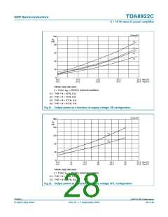
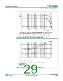
010aaa577
(1)
40
Gv(cl)
(dB)
(2)
(3)
30
20
10
2
3
4
5
10
10
10
10
10
fi (Hz)
VDD = 30 V, VSS = −30 V, fosc = 350 kHz (external oscillator), Vi = 100 mV, Ci = 330 pF.
(1) 1 × 8 Ω BTL configuration; LLC = 15 µH, CLC = 680 nF, VDD = 25 V, VSS = −25 V.
(2) 2 × 8 Ω SE configuration; LLC = 33 µH, CLC = 330 nF, VDD = 30 V, VSS = −30 V.
(3) 2 × 6 Ω SE configuration; LLC = 33 µH, CLC = 330 nF, VDD = 30 V; VSS = −30 V.
Fig 23. Closed-loop voltage gain as a function of frequency
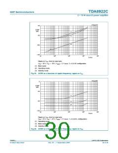
010aaa578
−20
SVRR
(dB)
(1)
−60
(2)
(3)
−100
−140
2
3
4
5
10
10
10
10
10
f (Hz)
i
Ripple on VDD, short on input pins.
VDD = 30 V, VSS = −30 V, Vripple = 2 V (p-p), 2 × 8 Ω SE configuration.
(1) Operating mode.
(2) Mute mode.
(3) Standby mode.
Fig 24. SVRR as a function of ripple frequency, ripple on VDD
TDA8922C_1
© NXP B.V. 2009. All rights reserved.
Product data sheet
Rev. 01 — 7 September 2009
29 of 40

 NXP [ NXP ]