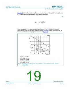
TDA8922C
NXP Semiconductors
2 × 75 W class-D power amplifier
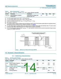
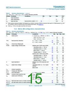
Table 9.
Dynamic characteristics …continued
VDD = 30 V; VSS = −30 V; Tamb = 25 °C; unless otherwise specified.
Symbol Parameter
Conditions
Min
Typ
Max
-
Unit
MΩ
pF
Zi
input impedance
1
-
-
-
-
Ci
tr(i)
input capacitance
input rise time
15
[2]
from SGCN to SGND + 5 V
-
100
ns
[1] When using an external oscillator, the frequency ftrack (500 kHz minimum, 900 kHz maximum) will result in a PWM frequency fosc (250
kHz minimum, 450 kHz maximum) due to the internal clock divider; see Section 8.2.
[2] When tr(i) > 100 ns, the output noise floor will increase.
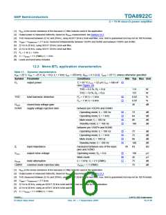
12.2 Stereo SE configuration characteristics
Table 10. Dynamic characteristics
VDD = 30 V; VSS = −30 V; RL = 6 Ω; fi = 1 kHz; fosc = 350 kHz; Rs(L) < 0.1 Ω[1]; Tamb = 25 °C; unless otherwise specified.
Symbol Parameter
Conditions
Min Typ Max Unit
[2]
Po
output power
L = 22 µH; CLC = 680 nF; Tj = 85 °C
THD = 0.5 %; RL = 6 Ω
THD = 10 %; RL = 6 Ω
Po = 1 W; fi = 1 kHz
-
58
75
-
-
W
W
%
%
dB
-
[3]
[3]
THD
total harmonic distortion
-
0.02 -
0.05 -
Po = 1 W; fi = 6 kHz
-
Gv(cl)
closed-loop voltage gain
29
30
31
SVRR
supply voltage rejection ratio
between pins VDDPn and SGND
Operating mode; fi = 100 Hz
Operating mode; fi = 1 kHz
Mute mode; fi = 100 Hz
[4]
[4]
[4]
[4]
-
-
-
-
72
-
-
-
-
dB
dB
dB
dB
55
80
Standby mode; fi = 100 Hz
between pins VSSPn and SGND
Operating mode; fi = 100 Hz
Operating mode; fi = 1 kHz
Mute mode; fi = 100 Hz
116
[4]
[4]
[4]
[4]
-
72
60
-
-
-
-
-
dB
dB
dB
dB
kΩ
-
-
72
Standby mode; fi = 100 Hz
-
116
63
Zi
input impedance
between one of the input pins and
SGND
45
[5]
Vn(o)
output noise voltage
Operating mode; Rs = 0 Ω; inputs
-
160
-
µV
shorted
[6]
[7]
Mute mode
-
-
-
-
-
-
-
-
-
-
85
70
-
-
-
1
-
-
-
-
-
-
-
µV
dB
dB
dB
dB
%
αcs
channel separation
|∆Gv|
αmute
CMRR
ηpo
voltage gain difference
mute attenuation
[8]
fi = 1 kHz; Vi = 2 V (RMS)
Vi(CM) = 1 V (RMS)
SE, RL = 6 Ω
75
75
88
90
90
380
320
common mode rejection ratio
output power efficiency
SE, RL = 8 Ω
%
BTL, RL = 16 Ω
%
[9]
[9]
RDSon(hs) high-side drain-source on-state resistance
RDSon(ls) low-side drain-source on-state resistance
mΩ
mΩ
TDA8922C_1
© NXP B.V. 2009. All rights reserved.
Product data sheet
Rev. 01 — 7 September 2009
15 of 40

 NXP [ NXP ]