TDA8922C
NXP Semiconductors
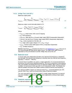
2 × 75 W class-D power amplifier
Table 8.
Static characteristics …continued
VDD = 30 V; VSS = −30 V; fosc = 350 kHz; Tamb = 25 °C; unless otherwise specified.
Symbol
Parameter
Conditions
Min
Typ
Max
Unit
[7]
Tact(th_fold) thermal foldback activation
temperature
closed loop SE voltage gain
reduced with 6 dB
-
153
-
°C
[1] VDD is the supply voltage on pins VDDP1, VDDP2 and VDDA.
[2] VSS is the supply voltage on pins VSSP1, VSSP2, VSSA and VSSD.
[3] Unbalance protection activated when VDDA > 2 × |VSSA| OR |VSSA| > 2 × VDDA
[4] With respect to SGND (0 V).
.
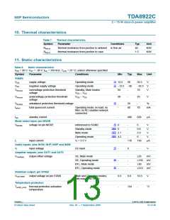
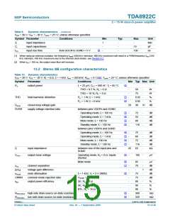
[5] The transition between Standby and Mute modes has hysteresis, while the slope of the transition between Mute and Operating modes is
determined by the time-constant of the RC network on pin MODE; see Figure 8.
[6] DC output offset voltage is gradually applied to the output during the transition between Mute and Operating modes. The slope caused
by any DC output offset is determined by the time-constant of the RC network on pin MODE.
[7] At a junction temperature of approximately Tact(th_fold) − 5 °C, gain reduction commences and at a junction temperature of approximately
Tact(th_prot), the amplifier switches off.
slope is directly related to the time-constant
of the RC network on the MODE pin
V
(V)
O
V
O(offset)(on)
Standby
Mute
On
V
O(offset)(mute)
0
0.8
2.1
2.9
4.2
5.5
V
(V)
MODE
010aaa585
Fig 8.
Behavior of mode selection pin MODE
12. Dynamic characteristics
12.1 Switching characteristics
Table 9.
Dynamic characteristics
VDD = 30 V; VSS = −30 V; Tamb = 25 °C; unless otherwise specified.
Symbol Parameter
Internal oscillator
Conditions
Min
Typ
Max
Unit
fosc(typ) typical oscillator frequency ROSC = 30.0 kΩ
fosc oscillator frequency
External oscillator input or frequency tracking; pin OSC
290
250
345
-
365
450
kHz
kHz
VOSC
Vtrip
voltage on pin OSC
trip voltage
HIGH-level
SGND + 4.5 SGND + 5
SGND + 6
V
-
SGND + 2.5 -
900
V
[1]
ftrack
tracking frequency
500
-
kHz
TDA8922C_1
© NXP B.V. 2009. All rights reserved.
Product data sheet
Rev. 01 — 7 September 2009
14 of 40

 NXP [ NXP ]