TDA8922C
NXP Semiconductors
2 × 75 W class-D power amplifier
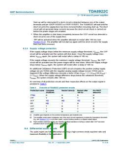
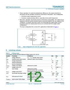
• Stereo operation: to avoid acoustical phase differences, the inputs should be in
anti-phase and the speakers should be connected in anti-phase. This configuration:
– minimizes power supply peak current
– minimizes supply pumping effects, especially at low audio frequencies
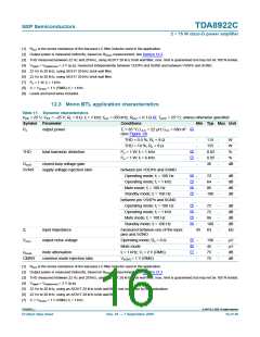
• Mono BTL operation: the inputs must be connected in anti-parallel. The output of one
channel is inverted and the speaker load is connected between the two outputs of the
TDA8922C. In practice (because of the OCP threshold) the output power can be
boosted to twice the output power that can be achieved with the single-ended
configuration.
The input configuration for a mono BTL application is illustrated in Figure 7.
OUT1
IN1P
IN1M
V
SGND
in
IN2P
IN2M
OUT2
power stage
mbl466
Fig 7. Input configuration for mono BTL application
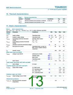
9. Limiting values
Table 6. Limiting values
In accordance with the Absolute Maximum Rating System (IEC 60134).
Symbol
∆V
Parameter
Conditions
DD − VSS; Standby, Mute modes
Min
-
Max
Unit
V
voltage difference
V
65
IORM
Tstg
repetitive peak output current maximum output current limiting
storage temperature
6
-
A
−55
−40
-
+150
+85
°C
°C
°C
V
Tamb
Tj
ambient temperature
junction temperature
150
VMODE
VOSC
VI
voltage on pin MODE
voltage on pin OSC
input voltage
referenced to SGND
0
6
0
SGND + 6
+5
V
referenced to SGND
−5
V
pins IN1P, IN1M, IN2P and IN2M
VPROT
VESD
voltage on pin PROT
referenced to voltage on pin VSSD
0
12
V
electrostatic discharge voltage Human Body Model (HBM)
Charged Device Model (CDM)
−2000 +2000
−500 +500
V
V
Iq(tot)
total quiescent current
Operating mode; no load; no filter
no RC-snubber network connected
-
70
mA
VPWM(p-p) peak-to-peak PWM voltage
on pins OUT1 and OUT2
-
120
V
TDA8922C_1
© NXP B.V. 2009. All rights reserved.
Product data sheet
Rev. 01 — 7 September 2009
12 of 40

 NXP [ NXP ]