TDA8920C
NXP Semiconductors
2 × 110 W class-D power amplifier
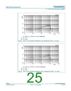
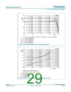
010aaa540
40
(1)
(2)
G
v(cl)
(dB)
(3)
(4)
30
20
10
2
3
4
5
10
10
10
10
10
f (Hz)
i
VP = ±30 V, fosc = 350 kHz, Vi = 100 mV, Ci = 330 pF, LLC = 15 µH, CLC = 680 nF.
(1) 1 × 8 Ω BTL configuration.
(2) 2 × 4 Ω SE configuration.
(3) 2 × 6 Ω SE configuration.
(4) 2 × 8 Ω SE configuration.
Fig 23. Closed-loop voltage gain as a function of frequency
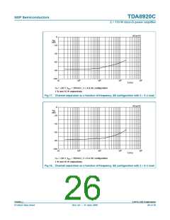
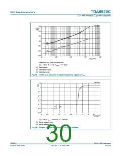
001aai710
−20
SVRR
(dB)
−40
−60
(1)
−80
(2)
−100
−120
−140
(3)
2
3
4
5
10
10
10
10
10
f
(Hz)
ripple
Ripple on VDD, short on input pins.
VP = ±30 V, RL = 4 Ω, Vripple = 2 V (p-p).
(1) Mute mode.
(2) Operating mode.
(3) Standby mode.
Fig 24. SVRR as a function of ripple frequency, ripple on VDD
TDA8920C_2
© NXP B.V. 2009. All rights reserved.
Product data sheet
Rev. 02 — 11 June 2009
29 of 39

 NXP [ NXP ]