LPC2212/2214
NXP Semiconductors
16/32-bit ARM microcontrollers
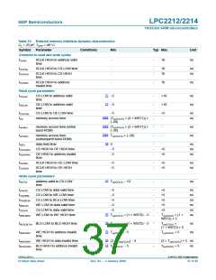
Table 10. External memory interface dynamic characteristics …continued
CL = 25 pF; Tamb = 40 °C.
Symbol
Parameter
Conditions
Min
Typ Max
Unit
[2]
tBLSHDNV BLS HIGH to data invalid
time
(2 × Tcy(CCLK)) − 5
-
-
-
-
-
-
-
(2 × Tcy(CCLK)) + 5 ns
tCHDV
XCLK HIGH to data valid
time
-
-
-
-
-
-
10
10
10
10
10
10
ns
ns
ns
ns
ns
ns
tCHWEL
tCHBLSL
tCHWEH
tCHBLSH
tCHDNV
XCLK HIGH to WE LOW
time
XCLK HIGH to BLS LOW
time
XCLK HIGH to WE HIGH
time
XCLK HIGH to BLS HIGH
time
XCLK HIGH to data invalid
time
[1] Except on initial access, in which case the address is set up Tcy(CCLK) earlier.
[2] Tcy(CCLK) = 1⁄CCLK.
[3] Latest of address valid, CS LOW, OE LOW to data valid.
[4] Address valid to data valid.
[5] Earliest of CS HIGH, OE HIGH, address change to data invalid.
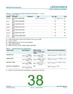
Table 11. Standard read access specifications
Access cycle
Max frequency
WST[1] setting
Memory access time requirement
WST ≥ 0; round up to
integer
standard read
2 + WST1
RAM + 20 ns
t
RAM + 20 ns
tRAM ≤ tcy(CCLK) × (2 + WST1) – 20 ns
f MAX
f MAX
f MAX
f MAX
≤
≤
≤
≤
--------------------------------
WST1 ≥
WST2 ≥
– 2
--------------------------------
tcy(CCLK)
t
standard write
1 + WST2
t
WRITE – tCYC + 5
tWRITE ≤ tcy(CCLK) × (1 + WST2) – 5 ns
tINIT ≤ tcy(CCLK) × (2 + WST1) – 20 ns
---------------------------------
-------------------------------------------
t
WRITE + 5 ns
tcy(CCLK)
burst read - initial
burst read - subsequent 3×
2 + WST1
tINIT + 20 ns
-------------------------------
WST1 ≥
– 2
-------------------------------
tINIT + 20 ns
tcy(CCLK)
N/A
1
t
ROM ≤ tcy(CCLK) – 20 ns
--------------------------------
tROM + 20 ns
[1] See the LPC2114/2124/2212/2214 User Manual for a description of the WSTn bits.
LPC2212_2214_4
© NXP B.V. 2008. All rights reserved.
Product data sheet
Rev. 04 — 3 January 2008
38 of 45

 NXP [ NXP ]