LPC2210/2220
NXP Semiconductors
16/32-bit ARM microcontrollers
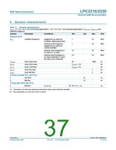
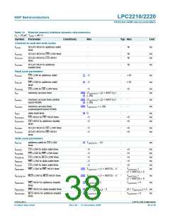
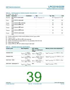
Table 12. ADC static characteristics
VDDA(3V3) = 2.5 V to 3.6 V; Tamb = −40 °C to +85 °C unless otherwise specified. ADC frequency 4.5 MHz.
Symbol
VIA
Parameter
Conditions
Min
Typ
Max
VDDA(3V3)
1
Unit
V
analog input voltage
analog input capacitance
differential linearity error
integral non-linearity
offset error
0
-
-
-
-
-
-
-
-
-
-
-
-
-
Cia
pF
[1][2][3]
[1][4]
ED
±1
LSB
LSB
LSB
%
EL(adj)
EO
±2
[1][5]
±3
[1][6]
EG
gain error
±0.5
±4
[1][7]
ET
absolute error
LSB
[1] Conditions: VSSA = 0 V, VDDA(3V3) = 3.3 V.
[2] The ADC is monotonic, there are no missing codes.
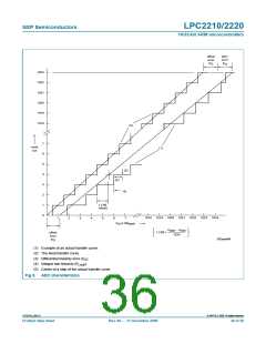
[3] The differential linearity error (ED) is the difference between the actual step width and the ideal step width. See Figure 5.
[4] The integral non-linearity (EL(adj)) is the peak difference between the center of the steps of the actual and the ideal transfer curve after
appropriate adjustment of gain and offset errors. See Figure 5.
[5] The offset error (EO) is the absolute difference between the straight line which fits the actual curve and the straight line which fits the
ideal curve. See Figure 5.
[6] The gain error (EG) is the relative difference in percent between the straight line fitting the actual transfer curve after removing offset
error, and the straight line which fits the ideal transfer curve. See Figure 5.
[7] The absolute voltage error (ET) is the maximum difference between the center of the steps of the actual transfer curve of the
non-calibrated ADC and the ideal transfer curve. See Figure 5.
LPC2210_2220_6
© NXP B.V. 2008. All rights reserved.
Product data sheet
Rev. 06 — 11 December 2008
35 of 50

 NXP [ NXP ]