LPC2210/2220
NXP Semiconductors
16/32-bit ARM microcontrollers
Table 14. External memory interface dynamic characteristics …continued
CL = 25 pF; Tamb = 40 °C.
Symbol
Parameter
Conditions
Min
Typ Max
Unit
[2]
tBLSHDNV BLS HIGH to data invalid
time
(2 × Tcy(CCLK)) − 5
-
(2 × Tcy(CCLK)) + 5 ns
tCHDV
XCLK HIGH to data valid
time
-
-
10
ns
tCHWEL
tCHBLSL
XCLK HIGH to WE LOW time
-
-
-
-
10
10
ns
ns
XCLK HIGH to BLS LOW
time
tCHWEH
tCHBLSH
tCHDNV
XCLK HIGH to WE HIGH
time
-
-
-
-
-
-
10
10
10
ns
ns
ns
XCLK HIGH to BLS HIGH
time
XCLK HIGH to data invalid
time
[1] Except on initial access, in which case the address is set up Tcy(CCLK) earlier.
[2] Tcy(CCLK) = 1⁄CCLK
.
[3] Latest of address valid, CS LOW, OE LOW to data valid.
[4] See the LPC2210/20 user manual UM10114_1 for a description of the WSTn bits.
[5] Address valid to data valid.
[6] Earliest of CS HIGH, OE HIGH, address change to data invalid.
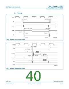
Table 15. Standard read access specifications
Access cycle
Max frequency
WST setting
Memory access time requirement
WST ≥ 0; round up to
integer
standard read
2 + WST1
RAM + 20 ns
t
RAM + 20 ns
tRAM ≤ tcy(CCLK) × (2 + WST1) – 20 ns
f MAX
f MAX
f MAX
f MAX
≤
≤
≤
≤
--------------------------------
WST1 ≥
WST2 ≥
– 2
--------------------------------
tcy(CCLK)
t
standard write
1 + WST2
t
WRITE – tCYC + 5
tWRITE ≤ tcy(CCLK) × (1 + WST2) – 5 ns
tINIT ≤ tcy(CCLK) × (2 + WST1) – 20 ns
---------------------------------
-------------------------------------------
t
WRITE + 5 ns
tcy(CCLK)
burst read - initial
burst read - subsequent 3×
2 + WST1
tINIT + 20 ns
-------------------------------
WST1 ≥
– 2
-------------------------------
tINIT + 20 ns
tcy(CCLK)
N/A
1
t
ROM ≤ tcy(CCLK) – 20 ns
--------------------------------
tROM + 20 ns
LPC2210_2220_6
© NXP B.V. 2008. All rights reserved.
Product data sheet
Rev. 06 — 11 December 2008
39 of 50

 NXP [ NXP ]