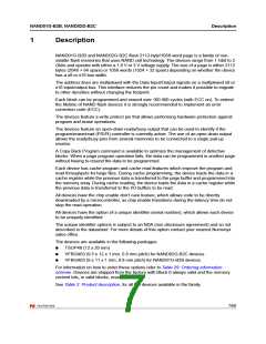
NAND01G-B2B, NAND02G-B2C
Description
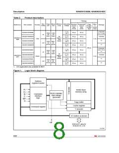
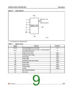
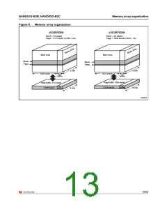
Figure 2.
Logic diagram
V
DD
I/O8-I/O15, x16
E
R
I/O0-I/O7, x8/x16
W
NAND01G-B2B
NAND02G-B2C
RB
AL
CL
WP
V
SS
AI13101
1. x16 organization only available for MCP.
Table 3.
Signal names
Signal
Function
Direction
I/O8-15
I/O0-7
Data input/outputs for x16 devices
I/O
I/O
Data input/outputs, address inputs, or command inputs
for x8 and x16 devices
AL
CL
E
Address Latch Enable
Command Latch Enable
Chip Enable
Input
Input
Input
Input
Output
Input
Input
Supply
Supply
–
R
Read Enable
RB
W
Ready/Busy (open-drain output)
Write Enable
WP
VDD
VSS
NC
DU
Write Protect
Supply voltage
Ground
Not connected internally
Do not use
–
9/60

 NUMONYX [ NUMONYX B.V ]