NAND01G-B2B, NAND02G-B2C
Description
1
Description
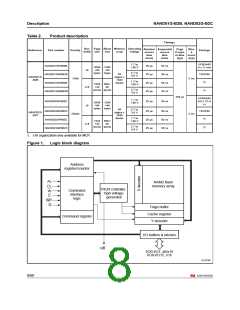
NAND01G-B2B and NAND02G-B2C flash 2112-byte/1056-word page is a family of non-
volatile flash memories that uses NAND cell technology. The devices range from 1 Gbit to 2
Gbits and operate with either a 1.8 V or 3 V voltage supply. The size of a page is either 2112
bytes (2048 + 64 spare) or 1056 words (1024 + 32 spare) depending on whether the device
has a x8 or x16 bus width.
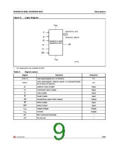
The address lines are multiplexed with the Data Input/Output signals on a multiplexed x8 or
x16 input/output bus. This interface reduces the pin count and makes it possible to migrate
to other densities without changing the footprint.
Each block can be programmed and erased over 100 000 cycles (with ECC on). To extend
the lifetime of NAND flash devices it is strongly recommended to implement an error
correction code (ECC).
The devices feature a write protect pin that allows performing hardware protection against
program and erase operations.
The devices feature an open-drain ready/busy output that can be used to identify if the
program/erase/read (P/E/R) controller is currently active. The use of an open-drain output
allows the ready/busy pins from several memories to be connected to a single pull-up
resistor.
A Copy Back Program command is available to optimize the management of defective
blocks. When a page program operation fails, the data can be programmed in another page
without having to resend the data to be programmed.
Each device has cache program and cache read features which improve the program and
read throughputs for large files. During cache programming, the device loads the data in a
cache register while the previous data is transferred to the page buffer and programmed into
the memory array. During cache reading, the device loads the data in a cache register while
the previous data is transferred to the I/O buffers to be read.
All devices have the chip enable don’t care feature, which allows code to be directly
downloaded by a microcontroller, as chip enable transitions during the latency time do not
stop the read operation.
All devices have the option of a unique identifier (serial number), which allows each device
to be uniquely identified.
The unique identifier options is subject to an NDA (non disclosure agreement) and so not
described in the datasheet. For more details of this option contact your nearest Numonyx
sales office.
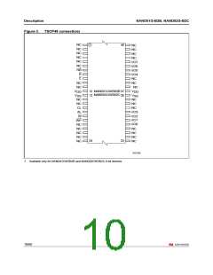
The devices are available in the following packages:
■
■
■
TSOP48 (12 x 20 mm)
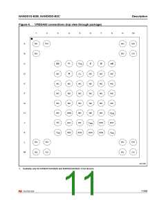
VFBGA63 (9.5 x 12 x 1 mm, 0.8 mm pitch) for NAND02G-B2C devices
VFBGA63 (9 x 11 x 1 mm, 0.8 mm pitch) for NAND01G-B2B devices.
For information on how to order these options refer to Table 29: Ordering information
scheme. Devices are shipped from the factory with Block 0 always valid and the memory
content bits, in valid blocks, erased to ’1’.
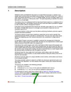
See Table 2: Product description, for all the devices available in the family.
7/60

 NUMONYX [ NUMONYX B.V ]