M25PX64
Instructions
6.14
Write to lock register (WRLR)
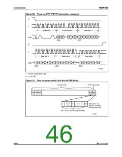
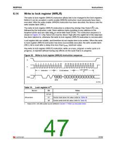
The write to lock register (WRLR) instruction allows bits to be changed in the lock registers.
Before it can be accepted, a write enable (WREN) instruction must previously have been
executed. After the write enable (WREN) instruction has been decoded, the device sets the
write enable latch (WEL).
The write to lock register (WRLR) instruction is entered by driving Chip Select (S) Low,
followed by the instruction code, three address bytes (pointing to any address in the
targeted sector and one data byte on serial data input (DQ0). The instruction sequence is
shown in Figure 22. Chip Select (S) must be driven High after the eighth bit of the data byte
has been latched in, otherwise the write to lock register (WRLR) instruction is not executed.
Lock register bits are volatile, and therefore do not require time to be written. When the write
to lock register (WRLR) instruction has been successfully executed, the write enable latch
(WEL) bit is reset after a delay time less than tSHSL minimum value.
Any write to lock register (WRLR) instruction, while an erase, program or write cycle is in
progress, is rejected without having any effects on the cycle that is in progress.
Figure 22. Write to lock register (WRLR) instruction sequence
S
0
1
2
3
4
5
6
7
8
9
10
28 29 30 31 32 33 34 35 36 37 38 39
C
Lock register
in
Instruction
24-bit address
23 22 21
MSB
3
2
1
0
7
6
5
4
3
2
0
1
DQ0
MSB
AI13740
Table 10. Lock register in(1)
Sector
Bit
Value
‘0’
b7-b2
b1
All sectors
Sector lock down bit value (refer to Table 9)
Sector write lock bit value (refer to Table 9)
b0
1. Values of (b1, b0) after power-up are defined in Section 7: Power-up and power-down.
47/68

 NUMONYX [ NUMONYX B.V ]