M25PX64
Instructions
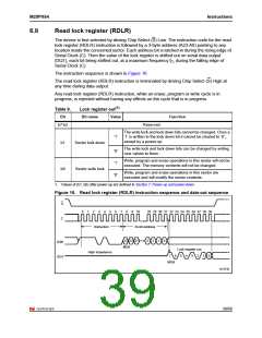
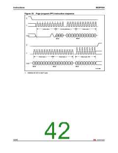
6.12
Dual input fast program (DIFP)
The dual input fast program (DIFP) instruction is very similar to the page program (PP)
instruction, except that the data are entered on two pins (pin DQ0 and pin DQ1) instead of
only one. Inputting the data on two pins instead of one doubles the data transfer bandwidth
compared to the page program (PP) instruction.
The dual input fast program (DIFP) instruction is entered by driving Chip Select (S) Low,
followed by the instruction code, three address bytes and at least one data byte on serial
data input (DQ0).
If the 8 least significant address bits (A7-A0) are not all zero, all transmitted data that goes
beyond the end of the current page are programmed from the start address of the same
page (from the address whose 8 least significant bits (A7-A0) are all zero). Chip Select (S)
must be driven Low for the entire duration of the sequence.
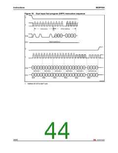
The instruction sequence is shown in Figure 19.
If more than 256 bytes are sent to the device, previously latched data are discarded and the
last 256 data bytes are guaranteed to be programmed correctly within the same page. If less
than 256 data bytes are sent to device, they are correctly programmed at the requested
addresses without having any effects on the other bytes in the same page.
For optimized timings, it is recommended to use the dual input fast program (DIFP)
instruction to program all consecutive targeted bytes in a single sequence rather to using
several dual input fast program (DIFP) sequences each containing only a few bytes (see
Table 17: AC characteristics).
Chip Select (S) must be driven High after the eighth bit of the last data byte has been
latched in, otherwise the dual input fast program (DIFP) instruction is not executed.
As soon as Chip Select (S) is driven High, the self-timed page program cycle (whose
duration is tPP) is initiated. While the dual input fast program (DIFP) cycle is in progress, the
status register may be read to check the value of the write in progress (WIP) bit. The write in
progress (WIP) bit is 1 during the self-timed page program cycle, and 0 when it is
completed. At some unspecified time before the cycle is completed, the write enable latch
(WEL) bit is reset.
A dual input fast program (DIFP) instruction applied to a page that is protected by the block
protect (BP2, BP1, BP0) bits (see Table 2 and Table 3) is not executed.
43/68

 NUMONYX [ NUMONYX B.V ]