Instructions
M25PX64
6.15
Subsector erase (SSE)
The subsector erase (SSE) instruction sets to ‘1’ (FFh) all bits inside the chosen subsector.
Before it can be accepted, a write enable (WREN) instruction must previously have been
executed. After the write enable (WREN) instruction has been decoded, the device sets the
write enable latch (WEL).
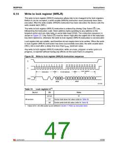
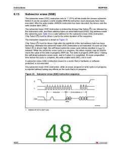
The subsector erase (SSE) instruction is entered by driving Chip Select (S) Low, followed by
the instruction code, and three address bytes on serial data input (DQ0). Any address inside
the subsector (see Table 4) is a valid address for the subsector erase (SSE) instruction.
Chip Select (S) must be driven Low for the entire duration of the sequence.
The instruction sequence is shown in Figure 23.
Chip Select (S) must be driven High after the eighth bit of the last address byte has been
latched in, otherwise the subsector erase (SSE) instruction is not executed. As soon as Chip
Select (S) is driven High, the self-timed subsector erase cycle (whose duration is tSSE) is
initiated. While the subsector erase cycle is in progress, the status register may be read to
check the value of the write in progress (WIP) bit. The write in progress (WIP) bit is 1 during
the self-timed subsector erase cycle, and is 0 when it is completed. At some unspecified
time before the cycle is complete, the write enable latch (WEL) bit is reset.
A subsector erase (SSE) instruction issued to a sector that is hardware or software
protected, is not executed.
Any subsector erase (SSE) instruction, while an erase, program or write cycle is in progress,
is rejected without having any effects on the cycle that is in progress.
Figure 23. Subsector erase (SSE) instruction sequence
S
0
1
2
3
4
5
6
7
8
9
29 30 31
C
Instruction
24-bit address (1)
2
0
1
23 22
MSB
DQ0
AI13741b
1. Address bit A23 is don’t care.
48/68

 NUMONYX [ NUMONYX B.V ]