M25PX64
DC and AC parameters
Table 17. AC characteristics(1) (continued)
Test conditions specified in Table 13 and Table 14
Symbol
Alt.
Parameter
Min
Typ(2)
Max Unit
tW
Write status register cycle time
Page program cycle time (256 bytes)
Page program cycle time (n bytes)
Program OTP cycle time (64 bytes)
Subsector erase cycle time
1.3
15
ms
ms
0.8
(8)
tPP
int(n/8) × 0.025(9)
5
0.2
70
ms
ms
s
tSSE
tSE
150
3
Sector erase cycle time
0.7
68
tBE
Bulk erase cycle time
160
s
1. Preliminary data.
2. Typical values given for TA = 25° C.
3. CH + tCL must be greater than or equal to 1/ fC.
t
4. Value guaranteed by characterization, not 100% tested in production.
5. Expressed as a slew-rate.
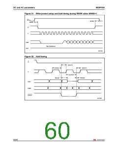
6. Only applicable as a constraint for a WRSR instruction when SRWD is set to ‘1’.
7. PPH should be kept at a valid level until the program or erase operation has completed and its result
V
(success or failure) is known. Avoid applying VPPH to the W/VPP pin during Bulk Erase.
8. When using the page program (PP) instruction to program consecutive bytes, optimized timings are
obtained with one sequence including all the bytes versus several sequences of only a few bytes (1 ≤ n ≤
256).
9. int(A) corresponds to the upper integer part of A. For example int(12/8) = 2, int(32/8) = 4 int(15.3) =16.
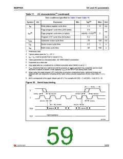
Figure 30. Serial input timing
tSHSL
S
tCHSL
tSLCH
tCHSH
tSHCH
C
tDVCH
tCHCL
tCHDX
tCLCH
MSB IN
LSB IN
DQ0
DQ1
High Impedance
AI13728
59/68

 NUMONYX [ NUMONYX B.V ]