®
Numonyx™ StrataFlash Embedded Memory (J3-65nm)
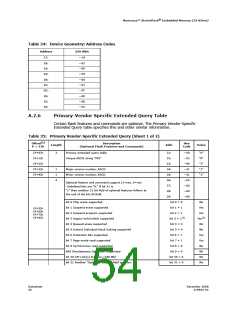
Table 35: Primary Vendor-Specific Extended Query (Sheet 2 of 2)
(1)
Offset
Description
(Optional Flash Features and Commands)
Hex
Code
Length
Add.
Value
P = 31h
Supported functions after suspend: read Array, Status, Query
Other supported operations are:
bits 1–7 reserved; undefined bits are “0”
3A:
--01
(P+9)h
1
bit 0 Program supported after erase suspend
Block Status Register mask
bit 0 = 1
Yes
3B:
3C:
--01
--00
bits 2–15 are Reserved; undefined bits are “0”
bit 0 Block Lock-Bit Status register active
bit 1 Block Lock-Down Bit Status active
(P+A)h
(P+B)h
2
bit 0 = 1
bit 1 = 0
Yes
No
V
logic supply highest performance program/erase voltage
bits 0–3 BCD value in 100 mV
bits 4–7 BCD value in volts
CC
(P+C)h
1
1
3D:
--33
--00
3.3 V
0.0 V
V
optimum program/erase supply voltage
PEN
(P+D)h
bits 0–3 BCD value in 100 mV
bits 4–7 HEX value in volts
3E:
Note:
1.
2.
Future devices may not support the described “Legacy Lock/Unlock” function. Thus bit 3 would have a value of “0.”
Setting this bit, will lead to the extension of the CFI table.
Table 36: Protection Register Information
(1)
Offset
Description
(Optional Flash Features and Commands)
Hex
Code
Length
Add.
Value
P = 31h
Number of Protection register fields in JEDEC ID space.
“00h,” indicates that 256 protection bytes are available
(P+E)h
1
3F:
--01
01
Protection Field 1: Protection Description
This field describes user-available One Time Programmable (OTP)
protection register bytes. Some are pre-programmed with device-
unique serial numbers. Others are user-programmable. Bits 0-15 point
to the protection register lock byte, the section’s first byte. The
following bytes are factory pre-programmed and user-programmable.
40:
41:
42:
43:
--80
--00
--03
--03
80h
00h
8bytes
8bytes
(P+F)h
(P+10)h
(P+11)h
(P+12)h
4
bits 0-7 = Lock/bytes JEDEC-plane physical low address
bits 8-15 = Lock/bytes JEDEC-plane physical high address
n
n
bits 16-23 = “n” such that 2 = factory pre-programmed bytes
bits 24-31 = “n” such that 2 = user-programmable bytes
Note:
1.
The variable P is a pointer which is defined at CFI offset 15h.
December 2008
319942-02
Datasheet
55

 NUMONYX [ NUMONYX B.V ]