®
Numonyx™ StrataFlash Embedded Memory (J3-65nm)
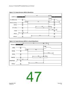
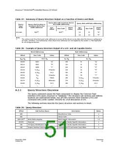
Table 27: Summary of Query Structure Output as a Function of Device and Mode
Query data with maximum device
Query data with byte addressing
bus width addressing
Device
Type/
Mode
Query start location in
maximum device bus
width addresses
Hex
Offset
ASCII
Value
Hex
Offset
ASCII
Value
Hex Code
Hex Code
(1)
(1)
x8 mode
N/A
N/A
21:
22:
51
52
“Q”
“R”
Note:
1.
The system must drive the lowest order addresses to access all the device's array data when the device is configured in
x8 mode. Therefore, word addressing, where these lower addresses are not toggled by the system, is "Not Applicable"
for x8-configured devices.
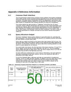
Table 28: Example of Query Structure Output of a x16- and x8-Capable Device
Word Addressing
Hex Code
Byte Addressing
Hex Code
Offset
–A
Value
Offset
Value
A
D15–D
A –A
7
D –D
7 0
15
0
0
0
0010h
0011h
0012h
0013h
0014h
0015h
0016h
0017h
0018h
...
0051
0052
0059
“Q”
“R”
20h
21h
22h
23h
24h
25h
26h
27h
28h
...
51
51
“Q”
“Q”
“Y”
52
“R”
P_ID
PrVendor
ID #
52
“R”
LO
P_ID
59
“Y”
HI
P
PrVendor
TblAdr
AltVendor
ID #
59
“Y”
LO
P
P_ID
P_ID
PrVendor
PrVendor
ID #
...
HI
LO
LO
A_ID
LO
A_ID
...
P_ID
HI
HI
...
...
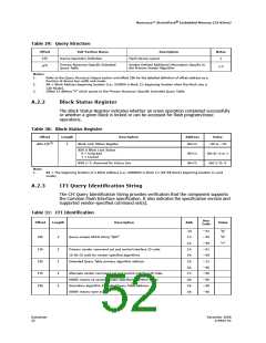
A.2.1
Query Structure Overview
The Query command causes the flash component to display the Common Flash
Interface (CFI) Query structure or “database.” The structure sub-sections and address
locations are summarized below. See AP-646 Common Flash Interface (CFI) and
Command Sets (order number 292204) for a full description of CFI.
The following sections describe the Query structure sub-sections in detail.
Table 29: Query Structure
Offset
Sub-Section Name
Description
Notes
00h
01h
Manufacturer Code
Device Code
1
1
(BA+2)h(2)
04-0Fh
10h
Block Status Register
Reserved
Block-Specific Information
1,2
1
Reserved for Vendor-Specific Information
Reserved for Vendor-Specific Information
Command Set ID and Vendor Data Offset
CFI Query Identification String
System Interface Information
1
1Bh
1
December 2008
319942-02
Datasheet
51

 NUMONYX [ NUMONYX B.V ]