®
Numonyx™ StrataFlash Embedded Memory (J3-65nm)
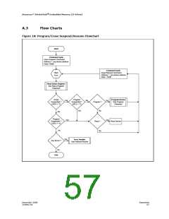
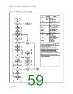
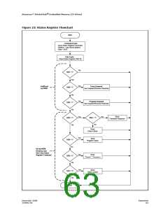
Figure 19: Buffer Program Flowchart
Bus
Command
Comments
Operation
Write to
Buffer
Data = E8H
Write
Read
Addr = Block Address
Start
SR.7 = Valid
Addr = Block Address
Device
Check SR.7
Use Single Word
Supports Buffer
Standby
1 = Device WSM is Busy
0 = Device WSM is Ready
No
Programming
Writes?
Yes
Data = N-1 = Word Count
N = 0 corresponds to count = 1
Addr = Block Address
Write
Set Timeout or
Loop Counter
(Notes1, 2)
Write
Data = Write Buffer Data
Addr = Start Address
(Notes3, 4)
Get Next
Target Address
Write
Data = Write Buffer Data
Addr = Block Address
(Notes5, 6)
Issue Write to Buffer
Command E8h and
Block Address
Program
Confirm
Data = D0H
Write
Read
Addr = Block Address
Status register Data
CE# and OE# low updates SR
Addr = Block Address
Read Status Register
(at Block Address)
Check SR.7
No
Standby
1 = WSM Ready
0 = WSM Busy
Timeout
or Count
Expired?
0 = No
Is WSM Ready?
SR.7 =
1. Word count values on DQ0-DQ7 are loaded into the Count
register. Count ranges for this device are N = 0000h to 0001Fh.
2. The device outputs the status register when read.
3. Write Buffer contents will be programmed at the device start
address or destination flash address.
Yes
1 = Yes
Write Word Count,
Block Address
4. Align the start address on a Write Buffer boundary for
maximum programming performance(i.e., A4–A0 of the start
address = 0).
Write Buffer Data,
Start Address
5. The device aborts the Buffered Program command if the
current address is outside the original block address.
6. The Status register indicates an "improper command
sequence" if the Buffered Program command is aborted. Follow
this with a Clear Status Register command.
X = X + 1
Write Buffer Data,
Block Address
X = 0
Full status check can be done after all erase and write
sequences complete. Write FFh after the last operation to reset
the device to read array mode.
No
No
Abort Bufferred
Program?
X = N?
Yes
Yes
Write Confirm D0h
and Block Address
Write to another
Block Address
Buffered Program
Aborted
Read Status Register
No
Suspend
Program
Loop
Yes
0
Suspend
Program
SR.7 =?
Full Status
Check if Desired
1
Yes
Another Buffered
Programming?
No
Program Complete
December 2008
319942-02
Datasheet
59

 NUMONYX [ NUMONYX B.V ]