®
Numonyx™ StrataFlash Embedded Memory (J3-65nm)
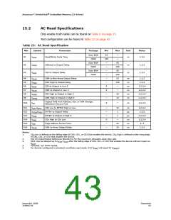
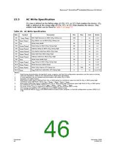
15.3
AC Write Specification
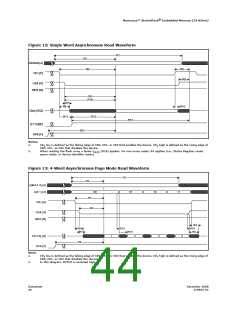
CEX low is defined as the falling edge of CE0, CE1, or CE2 that enables the device. CEX
high is defined at the rising edge of CE0, CE1, or CE2 that disables the device. Chip
enable truth table can be found in Table 6 on page 15
Table 24: AC Write Specification
Nbr.
Symbol
(t
Parameter
RP# High Recovery to WE# (CE ) Going Low
Min
Max
Unit
Notes
W1
W2
t
)
150
0
—
—
ns
ns
ns
ns
ns
ns
ns
ns
ns
ns
ns
ns
ns
1,2,3
1,2,4
1,2,4
1,2
PHWL PHEL
X
t
t
t
t
t
t
t
t
t
t
t
t
(t
)
CE (WE#) Low to WE# (CE ) Going Low
ELWL
WP
WLEL
X
X
W3
Write Pulse Width
50
50
50
0
—
W4
(t
)
Data Setup to WE# (CE ) Going High
—
DVWH DVEH
X
W5
(t
)
Address Setup to WE# (CE ) Going High
—
1,2
AVWH AVEH
X
W6
(t
)
CE (WE#) Hold from WE# (CE ) High
—
1,2,
WHEH
WHDX
EHWH
X
X
W7
(t
)
Data Hold from WE# (CE ) High
0
—
1,2,
EHDX
X
W8
(t
)
Address Hold from WE# (CE ) High
X
0
—
1,2,
WHAX EHAX
WPH
W9
Write Pulse Width High
20
0
—
1,2,5
1,2,3
1,2,6
1,2,7
1,2,3,7,8
W11
W14
W13
W15
(t
)
)
V
Setup to WE# (CE ) Going High
—
VPWH
VPEH
PEN
X
(t
Write Recovery before Read
WE# (CE ) High to STS Going Low
0
—
WHGL EHGL
(t
)
—
0
500
—
WHRL EHRL
X
V
Hold from Valid SRD, STS Going High
PEN
QVVL
Notes:
1.
Read timing characteristics during block erase, program, and lock-bit configuration operations are the same as during
read-only operations. Refer to AC Characteristics–Read-Only Operations.
2.
3.
4.
A write operation can be initiated and terminated with either CE or WE#.
X
Sampled, not 100% tested.
Write pulse width (t ) is defined from CE or WE# going low (whichever goes low last) to CE or WE# going high
WP
X
X
(whichever goes high first). Hence, t
= t
= t
X
WHWL
WHGL
= t
= t
.
WP
WLWH
ELEH
WLEH
ELWH
5.
Write pulse width high (t
low (whichever goes low first). Hence, t
) is defined from CE or WE# going high (whichever goes high first) to CE or WE# going
WPH
X
= t
= t
= t
= t
.
WPH
EHEL
WHEL
EHWL
6.
7.
8.
For array access, t
is required in addition to t
for any accesses after a write.
AVQV
STS timings are based on STS configured in its RY/BY# default mode.
V
should be held at V
until determination of block erase, program, or lock-bit configuration success (SR[5:3,1]
PEN
PENH
= 0).
Datasheet
46
December 2008
319942-02

 NUMONYX [ NUMONYX B.V ]