®
Numonyx™ StrataFlash Embedded Memory (J3-65nm)
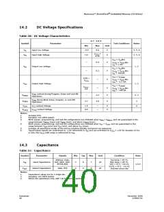
14.2
DC Voltage Specifications
Table 20: DC Voltage Characteristics
2.7 - 3.6 V
Symbol
Parameter
Test Conditions
Notes
Min
Max
Unit
V
Input Low Voltage
Input High Voltage
–0.5
0.6
V
2, 5, 6
2, 5, 6
IL
V
+
CCQ
0.5V
V
2.0
—
V
V
IH
V
V
= V Min
CC
CC
0.4
= V
Min
Min
Min
CCQ
CCQ
I
= 2 mA
OL
V
Output Low Voltage
1, 2
OL
V
V
= V Min
CC
= V
= 100 µA
CC
—
0.2
—
V
V
V
CCQ
CCQ
I
OL
V
V
= V
CC
CCMIN
0.85 ×
= V
= –2.5 mA
CCQ
CCQ
V
CCQ
I
OH
V
Output High Voltage
1, 2
2, 3
OH
V
V
= V
CC
CCMIN
V
–
CCQ
0.2
—
= V
Min
CCQ
CCQ
I
= –100 µA
OH
V
Lockout during Program, Erase and Lock-Bit
PEN
V
—
2.2
3.6
V
V
PENLK
Operations
V
during Block Erase, Program, or Lock-Bit
PEN
V
2.7
3
4
PENH
Operations
V
V
V
Lockout Voltage
1.5
0.9
—
—
V
V
LKO
CC
V
Lockout Voltage
LKOQ
CCQ
Notes:
1.
2.
3.
Includes STS.
Sampled, not 100% tested.
Block erases, programming, and lock-bit configurations are inhibited when V
≤ V
, and not guaranteed in the
PEN
PENLK
range between V
(max) and V
(min), and above V
(max).
PENLK
PENH
PENH
4.
Block erases, programming, and lock-bit configurations are inhibited when V < V
, and not guaranteed in the
LKO
CC
range between V
(min) and V (min), and above V (max).
LKO
CC CC
5.
6.
Includes all operational modes of the device including standby and power-up sequences
Input/Output signals can undershoot to -1.0V referenced to V and can overshoot to V
+ 1.0V for duration of 2ns
CCQ
SS
or less, the V
valid range is referenced to V
.
CCQ
SS
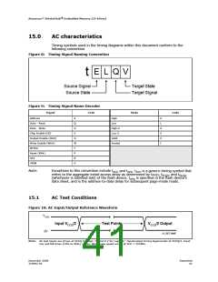
14.3
Capacitance
Table 21: Capacitance
Symbol
Parameter
Signals
Min
2
Typ
6
Max
Unit
pF
Condition
Note
Address, Data,
CE#, WE#, OE#,
BYTE#,RP#
Typ temp = 25 °C,
Max temp = 85 °C,
VCC = (0 V - 3.6 V),
VCCQ = (0 V - 3.6 V),
Discrete silicon die
C
Input Capacitance
Output Capacitance
7
5
IN
1,2,3
C
Data, STS
2
4
pF
OUT
Notes:
1.
2.
3.
Capacitance values are for a single die.
Sampled, not 100% tested.
Silicon die capacitance only, add 1 pF for discrete packages.
Datasheet
40
December 2008
319942-02

 NUMONYX [ NUMONYX B.V ]