®
Numonyx™ StrataFlash Embedded Memory (J3-65nm)
15.0
AC characteristics
Timing symbols used in the timing diagrams within this document conform to the
following convention
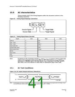
Figure 8: Timing Signal Naming Convention
E L Q V
t
Source Signal
Source State
Target State
Target Signal
Figure 9: Timing Signal Name Decoder
Signal
Code
State
Code
Address
A
Q
D
E
High
H
L
Data - Read
Data - Write
Low
High-Z
Low-Z
Valid
Z
X
V
I
Chip Enable (CE)
Output Enable (OE#)
Write Enable (WE#)
BYTE#
G
W
F
Invalid
Reset (RP#)
STS
P
R
V
VPEN
Note:
Exceptions to this convention include tACC and tAPA. tACC is a generic timing symbol that
refers to the aggregate initial-access delay as determined by tAVQV, tELQV, and tGLQV
(whichever is satisfied last) of the flash device. tAPA is specified in the flash device’s
data sheet, and is the address-to-data delay for subsequent page-mode reads.
15.1
AC Test Conditions
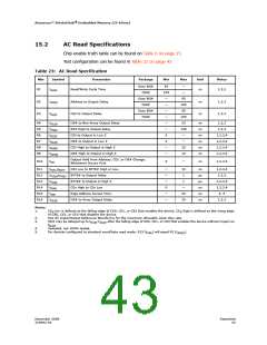
Figure 10: AC Input/Output Reference Waveform
VCCQ
Input VCCQ/2
Test Points
VCCQ/2 Output
0V
IO_REF.WMF
Note: AC test inputs are driven at VCCQ for Logic "1" and 0 V for Logic "0." Input/output timing begins/ends at VCCQ/2. Input
rise and fall times (10% to 90%) < 5 ns. Worst-case speed occurs at VCC = VCCMin.
December 2008
319942-02
Datasheet
41

 NUMONYX [ NUMONYX B.V ]