®
Numonyx™ StrataFlash Embedded Memory (J3-65nm)
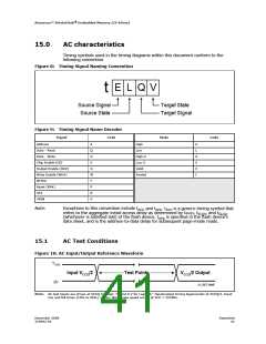
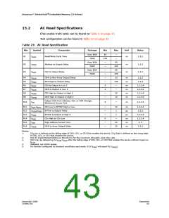
15.2
AC Read Specifications
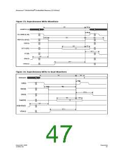
Chip enable truth table can be found on Table 6 on page 15
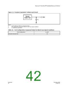
Test configuration can be found in Table 22 on page 42
Table 23: AC Read Specification
Nbr.
Symbol
Parameter
Package
Min
Max
Unit
Notes
Easy BGA
TSOP
95
105
—
—
—
—
—
—
0
—
—
R1
t
t
t
Read/Write Cycle Time
ns
1,2,3
AVAV
Easy BGA
TSOP
95
105
95
105
25
150
—
R2
R3
Address to Output Delay
CEX to Output Delay
ns
ns
1,2,3
1,2,3
AVQV
ELQV
Easy BGA
TSOP
R4
R5
R6
R7
R8
R9
t
t
t
t
t
t
OE# to Non-Array Output Delay
RP# High to Output Delay
CEX to Output in Low Z
ns
ns
ns
ns
ns
ns
1,2,3
1,2,3
GLQV
PHQV
ELQX
GLQX
EHQZ
GHQZ
1,2,3,4
1,2,3,4
1,2,3,4
1,2,3,4
OE# to Output in Low Z
0
—
CEX High to Output in High Z
OE# High to Output in High Z
—
—
20
15
Output Hold from Address, CEX, or OE# Change,
Whichever Occurs First
R10
t
0
—
ns
1,2,3,4
OH
R11
R12
R13
R14
R15
R16
t
t
t
t
t
t
t
CEX Low to BYTE# High or Low
BYTE# to Output Delay
—
—
—
0
10
1
ns
µs
µs
ns
ns
ns
1,2,3,4
1,2,3
ELFL/ ELFH
t
FLQV/ FHQV
BYTE# to Output in High Z
CEx High to CEx Low
1
1,2,3,4
1,2,3,4
4, 5
FLQZ
EHEL
APA
—
25
25
Page Address Access Time
OE# to Array Output Delay
—
—
1,2,3
GLQV
Notes:
1.
CE low is defined as the falling edge of CE0, CE1, or CE2 that enables the device. CE high is defined as the rising edge
X
X
of CE0, CE1, or CE2 that disables the device
2.
3.
See AC Input/Output Reference Waveforms for the maximum allowable input slew rate.
OE# may be delayed up to t
ELQV
-t
after the falling edge of CE0, CE1, or CE2 that enables the device without impact on
ELQV GLQV
t
.
4.
5.
Sampled, not 100% tested.
For devices configured to standard word/byte read mode, R15 (t
) will equal R2 (t
).
AVQV
APA
December 2008
319942-02
Datasheet
43

 NUMONYX [ NUMONYX B.V ]