Numonyx™ Wireless Flash Memory (W18)
Table 31: Read Configuration Register Descriptions (Sheet 2 of 2)
Bit
Name
Description1
Notes
BW
Burst Wrap
0 = Wrap bursts within burst length set by CR[2:0]
1 = Don’t wrap accesses within burst length set by CR[2:0].(Default)
3
001 = 4-Word Burst
010 = 8-Word Burst
BL[2:0]
2-0
4
011 = 16-Word Burst
111 = Continuous Burst (Default)
Burst Length
Notes:
1.
2.
Undocumented combinations of bits are reserved by Numonyx for future implementations.
Synchronous and page read mode configurations affect reads from main blocks and parameter blocks. Status Register
and configuration reads support single read cycles. RCR[15]=1 disables configuration set by RCR[14:0].
Data is not ready when WAIT is asserted.
3.
4.
5.
6.
Set the synchronous burst length. In asynchronous page mode, the page size equals four words.
Set all reserved Read Configuration Register bits to zero.
Setting the Read Configuration Register for synchronous burst-mode with a latency count of 2 (RCR[13:11] = 010),
data hold for 2 clocks (RCR[9] = 1), and WAIT asserted one data cycle before delay (RCR[8] =1) is not supported.
14.1
Read Mode (RCR[15])
All partitions support two high-performance read configurations: synchronous burst
mode and asynchronous page mode (default). RCR[15] sets the read configuration to
one of these modes.
Status register, query, and identifier modes support only asynchronous and single-
synchronous read operations.
14.2
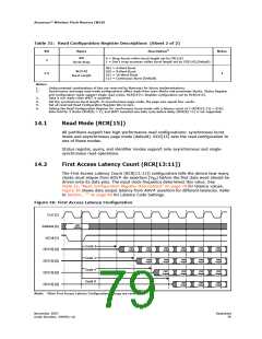
First Access Latency Count (RCR[13:11])
The First Access Latency Count (RCR[13:11]) configuration tells the device how many
clocks must elapse from ADV# de-assertion (VIH) before the first data word should be
driven onto its data pins. The input clock frequency determines this value. See
Table 31, “Read Configuration Register Descriptions” on page 78 for latency values.
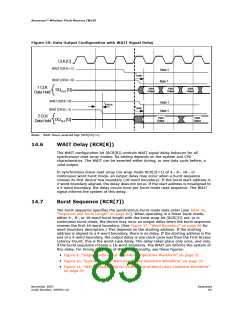
Figure 36 shows data output latency from ADV# assertion for different latencies. Refer
to Section , “” on page 80 for Latency Code Settings.
Figure 36: First Access Latency Configuration
CLK [C]
Valid
Address
Address [A]
ADV# [V]
Code 2
Valid
Output
Valid
Output
Valid
Output
Valid
Output
Valid
Output
Valid
Output
D[15:0] [Q]
D[15:0] [Q]
D[15:0] [Q]
D[15:0] [Q]
Code 3
Code 4
Code 5
Valid
Output
Valid
Output
Valid
Output
Valid
Output
Valid
Output
Valid
Output
Valid
Output
Valid
Output
Valid
Output
Valid
Output
Valid
Output
Valid
Output
Note: Other First Access Latency Configuration settings are reserved.
)
November 2007
Order Number: 290701-18
Datasheet
79

 NUMONYX [ NUMONYX B.V ]