Numonyx™ Wireless Flash Memory (W18)
14.0
Set Read Configuration Register
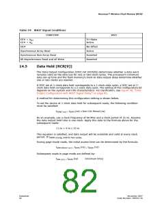
The Set Read Configuration Register (RCR) command sets the burst order, frequency
configuration, burst length, and other parameters.
A two-bus cycle command sequence initiates this operation. The Read Configuration
Register data is placed on the lower 16 bits of the address bus (A[15:0]) during both
bus cycles. The Set Read Configuration Register command is written along with the
configuration data (on the address bus). This is followed by a second write that
confirms the operation and again presents the Read Configuration Register data on the
address bus. The Read Configuration Register data is latched on the rising edge of
ADV#, CE#, or WE# (whichever occurs first). This command functions independently of
the applied VPP voltage. After executing this command, the device returns to read-array
mode. The Read Configuration Register’s contents can be examined by writing the Read
Identifier command and then reading location 05h. See Table 30 and Table 31.
Table 30: Read Configuration Register Summary
First Access Latency
Count
Burst Length
RM
15
R
LC2
13
LC1
12
LC0
11
WT
10
DOC
9
WC
8
BS
7
CC
6
R
5
R
4
BW
3
BL2
BL1
1
BL0
14
2
0
Table 31: Read Configuration Register Descriptions (Sheet 1 of 2)
Bit
Name
Description1
Notes
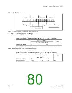
RM
Read Mode
0 = Synchronous Burst Reads Enabled
15
14
2
5
1 = Asynchronous Reads Enabled (Default)
Reserved
R
001 = Reserved
010 = Code 2
011 = Code 3
100 = Code 4
101 = Code 5
111 = Reserved (Default)
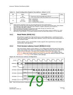
LC[2:0]
13-11
6
First Access Latency Count
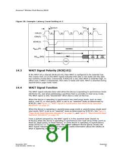
WT
0 = WAIT signal is asserted low
1 = WAIT signal is asserted high (Default)
10
9
3
6
6
WAIT Signal Polarity
DOC
0 = Hold Data for One Clock
1 = Hold Data for Two Clock (Default)
Data Output Configuration
0 = WAIT Asserted During Delay
1 = WAIT Asserted One Data Cycle before Delay (Default)
8
WC WAIT Configuration
BS
7
1 = Linear Burst Order (Default)
Burst Sequence
CC
0 = Burst Starts and Data Output on Falling Clock Edge
1 = Burst Starts and Data Output on Rising Clock Edge (Default)
6
Clock Configuration
5
4
R
R
Reserved
Reserved
5
5
Datasheet
78
November 2007
Order Number: 290701-18

 NUMONYX [ NUMONYX B.V ]