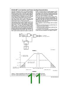
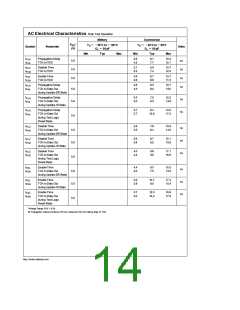
AC Operating Requirements Scan Test Operation
Military
Commercial
e b
a
e b
A
a
V
*
T
A
55 C to 125 C
§
T
40 C to 85 C
§
CC
§
§
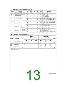
Symbol
Parameter
Units
e
e
(V)
C
50 pF
C
L
50 pF
L
Guaranteed Minimum
t
t
t
t
t
t
t
t
t
t
t
t
t
f
t
t
Setup Time
S
5.0
5.0
5.0
5.0
5.0
5.0
5.0
5.0
5.0
5.0
5.0
5.0
5.0
5.0
4.8
ns
ns
ns
ns
ns
ns
ns
ns
ns
ns
ns
ns
ns
MHz
Data to TCK (Note 1)
Hold Time
H
2.5
4.1
1.7
4.2
2.3
3.8
2.3
8.7
1.5
6.7
5.0
Data to TCK (Note 1)
Setup Time, H or L
S
G1, G2 to TCK (Note 2)
Hold Time, H or L
H
TCK to G1, G2 (Note 2)
Setup Time, H or L
S
DIR1, DIR2 to TCK (Note 4)
Hold Time, H or L
H
TCK to DIR1, DIR2 (Note 4)
Setup Time
S
Internal OE to TCK (Note 3)
Hold Time, H or L
H
TCK to Internal OE (Note 3)
Setup Time, H or L
TMS to TCK
S
Hold Time, H or L
TCK to TMS
H
Setup Time, H or L
TDI to TCK
S
Hold Time, H or L
TCK to TDI
H
Pulse Width TCK
H
L
10.2
8.5
W
max
PU
DN
Maximum TCK
50
Clock Frequency
Wait Time,
5.0
0.0
100
100
ns
Power Up to TCK
Power Down Delay
ms
g
*Voltage Range 5.0V 0.5V
All Input Timing Delays involving TCK are measured from the rising edge of TCK.
Note 1: Timing pertains to the TYPE1 BSR and TYPE2 BSR after the buffer (BSR 0–8, 9–17, 18–26, 27–35, 36–44, 45–53, 54–62, 63–71).
Note 2: Timing pertains to BSR 74 and 78 only.
Note 3: Timing pertains to BSR 72, 73, 76 and 77 only.
Note 4: Timing pertains to BSR 75 and 79 only.
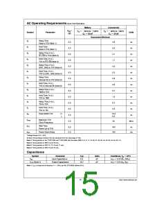
Capacitance
Symbol
e
25 C
Parameter
Typ
5.9
Units
pF
Conditions, T
§
0.0V (G , DIR )
n n
A
e
e
C
C
Input Capacitance
Output Capacitance
V
V
IN
CC
(Note 1)
13.7
pF
5.0V (A , B )
n n
I/O
CC
e
1 MHz, per MIL-STD-883B, Method 3012.
Note 1: C
is measured at frequency f
I/O
15
http://www.national.com

 NSC [ National Semiconductor ]