SCAN ABT Live Insertion and Power Cycling Characteristics
SCAN ABT is intended to serve in Live Insertion backplane
1
applications. It provides 2nd Level Isolation which indicates
flip-flop. To bring the device out of high impedance, the G
input must receive an inactive-to-active transition, a high-to-
n
that while external circuitry to control the output enable pin
is unnecessary, there may be a need to implement differen-
low transition on G in this case to change the state of the
n
flip-flop. With a low on the Q output of the flip-flop, the NOR
tial length backplane connector pins for V
and GND. As
gate is free to allow propagation of a G signal.
n
CC
well, pre-bias circuitry for backplane pins may be necessary
to avoid capacitive loading effects during live insertion.
During power-down, the Power-On-Reset circuitry will be-
come active and reset the flip-flop at approximately 1.8V
SCAN ABT provides control of output enable pins during
power cycling via the circuit in Figure A. It essentially con-
V
. Again, the Q output of the flip-flop returns to a high and
CC
disables the NOR gate from inputs from the G pin. The
n
device will then remain in high impedance for the remaining
trols the G pin until V
n
reaches a known level.
CC
ramp down from 1.8V to 0.0V V
.
CC
During power-up, when V ramps through the 0.0V to 0.7V
CC
range, all internal device circuitry is inactive, leaving output
and I/O pins of the device in high impedance. From approxi-
Some suggestions to help the designer with live insertion
issues:
mately 0.8V to 1.8V V , the Power-On-Reset circuitry,
CC
The G pin can float during power-up until the Power-On-
n
Reset circuitry becomes inactive.
#
(POR), in Figure A becomes active and maintains device
high impedance mode. The POR does this by providing a
low from its output that resets the flip-flop The output, Q, of
the flip-flop then goes high and disables the NOR gate from
The G pin can float on power-down only after the Pow-
n
er-On-Reset has become active.
#
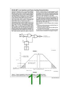
The description of the functionality of the Power-On-Reset
circuitry can best be described in the diagram of Figure B.
an incidental low input on the G pin. After 1.8V V , the
n CC
POR circuitry becomes inactive and ceases to control the
TL/F/11657–19
FIGURE A
TL/F/11657–20
FIGURE B
Section 7, ‘‘Design Consideration for Fault Tolerant Backplanes’’, Application Note AN-881.
1
SCAN ABT includes additional power-on reset circuitry not otherwise included in ABT devices.
11
http://www.national.com

 NSC [ National Semiconductor ]