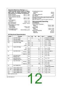
Absolute Maximum Ratings (Note 1)
If Military/Aerospace specified devices are required,
please contact the National Semiconductor Sales
Office/Distributors for availability and specifications.
DC Latchup Source Current
Commercial
Military
b
b
500 mA
300 mA
b
b
a
65 C to 150 C
Storage Temperature
Over Voltage Latchup (I/O)
ESD (HBM) Min.
10V
§
§
a
55 C to 125 C
Ambient Temperature under Bias
2000V
§
§
Note 1: Absolute maximum ratings are values beyond which the device may
be damaged or have its useful life impaired. Functional operation under
these conditions is not implied.
Junction Temperature under Bias
Ceramic
Plastic
b
b
a
55 C to 175 C
§
§
§
§
a
55 C to 150 C
Note 2: Either voltage limit or current limit is sufficient to protect inputs.
V
Pin Potential to
CC
Ground Pin
b
a
0.5V to 7.0V
Recommended Operating
Conditions
b
a
0.5V to 7.0V
Input Voltage (Note 2)
Input Current (Note 2)
b
a
30 mA to 5.0 mA
Free Air Ambient Temperature
Military
Commercial
Voltage Applied to Any Output
in the Disabled or
Power-Off State
b
b
a
55 C to 125 C
§
40 C to 85 C
§
a
§
§
b
a
0.5V to 5.5V
Supply Voltage
Military
Commercial
b
in the HIGH State
0.5V to V
CC
a
a
a
4.5V to 5.5V
Current Applied to Output
in LOW State (Max)
a
4.5V to 5.5V
Twice the Rated I (mA)
OL
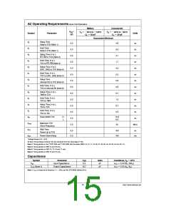
Minimum Input Edge Rate
Data Input
Enable Input
(DV/Dt)
50 mV/ns
20 mV/ns
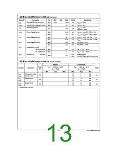
DC Electrical Characteristics
Symbol
Parameter
Input HIGH Voltage
V
Min
Typ
Max
Units
Conditions
CC
V
IH
2.0
V
V
V
V
V
V
Recognized HIGH Signal
Recognized LOW Signal
V
V
V
Input LOW Voltage
0.8
IL
b
e b
18 mA
Input Clamp Diode Voltage
Output HIGH Voltage
Min
Min
Min
Min
1.2
I
I
I
I
CD
OH
IN
e b
e b
e b
2.5
2.0
2.0
3 mA
OH
OH
OH
Mil
24 mA
32 mA
Comm
V
Output LOW Voltage
Input HIGH Current
OL
e
e
e
e
e
e
Mil
Min
Min
0.8
V
I
I
12 mA
OL
Comm
0.8
5
V
15 mA
OL
I
Max
Max
Max
mA
mA
mA
V
V
V
V
2.7V (Note 1)
IH
IN
IN
IN
IN
All Others
TMS, TDI
5
V
CC
V
CC
5
I
I
I
Input HIGH Current
Breakdown Test
7.0V
BVI
BVIT
IL
Max
Max
7
mA
mA
e
Input HIGH Current
V
5.5V
IN
100
Breakdown Test (I/O)
b
b
e
e
e
Input LOW Current
Max
Max
Max
5
5
mA
mA
mA
V
V
V
0.5V (Note 1)
0.0V
IN
IN
IN
All Others
TMS, TDI
b
385
0.0V
e
ID
V
ID
Input Leakage Test
I
1.9 mA
0.0
4.75
V
All Other Pins Grounded
a
e
e
e
e
I
I
I
I
I
Output Leakage Current
Output Leakage Current
Output Leakage Current
Output Leakage Current
Max
Max
Max
Max
50
mA
mA
mA
mA
V
OUT
V
OUT
V
OUT
V
OUT
2.7V
0.5V
2.7V
0.5V
IH
IL
OZH
a
b
I
50
OZL
50
OZH
OZL
b
50
Note 1: Guaranteed not tested.
http://www.national.com
12

 NSC [ National Semiconductor ]