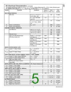
AC Electrical Characteristics
The following specifications apply for +2.8 VDC ≤V+ ≤ +3.8 VDC on SMBCLK and SMBData, unless otherwise specified. Bold-
face limits apply for TA = TJ = TMIN to TMAX; all other limits T = TJ = 25˚C. (Note 17)
A
Symbol
Parameter
Conditions
Typical
Limits
Units
(Note 9)
(Note 10)
(Limits)
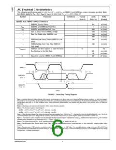
SERIAL BUS TIMING CHARACTERISTICS
t 1
trise
tfall
t 2
SMBCLK (Clock) Period
2.5
1
µs (min)
µs (max)
ns (max)
ns (min)
ns (min)
ns (max)
ns (min)
SMBCLK and SMBData Rise Time
SMBCLK and SMBData Fall Time
Data In Setup Time to SMBCLK High
Data Out Stable After SMBCLK Low
300
100
100
300
100
t 3
t 4
t 5
SMBData Low Setup Time to SMBCLK Low
(start)
SMBData High Hold Time After SMBCLK
High (stop)
100
ns (min)
tTIMEOUT
SMBCLK low time required to reset the Serial
Bus Interface to the Idle State
31
ms
25
35
80
ms (min)
ms (max)
pF (max)
CL
Capacitive Load on SMBCLK and SMBData
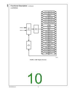
10099504
FIGURE 1. Serial Bus Timing Diagram
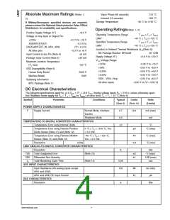
Note 1: Absolute Maximum Ratings indicate limits beyond which damage to the device may occur. Operating Ratings indicate conditions for which the device is
functional, but do not guarantee specific performance limits. For guaranteed specifications and test conditions, see the Electrical Characteristics. The guaranteed
specifications apply only for the test conditions listed. Some performance characteristics may degrade when the device is not operated under the listed test
conditions.
Note 2: All voltages are measured with respect to GND, unless otherwise specified.
Note 3: The Absolute maximum input range for :
+
+2.5Vin - −0.3 V to (1.4 x V + 0.42 V or 6 V, whichever is smaller
+
+3.3Vin - −0.3 V to (1.8 x V + 0.55 V or 6 V, whichever is smaller.
+
<
>
V
Note 4: When the input voltage (V ) at any pin exceeds the power supplies (V
GND or V
IN
), the current at that pin should be limited to 5 mA. The 20 mA
IN
IN
maximum package input current rating limits the number of pins that can safely exceed the power supplies with an input current of 5 mA to four.
Note 5: The maximum power dissipation must be derated at elevated temperatures and is dictated by T max, θ and the ambient temperature, T . The maximum
J
JA
A
allowable power dissipation at any temperature is P = (T max−T )/θ .
D
J
A
JA
Note 6: The human body model is a 100 pF capacitor discharged through a 1.5 kΩ resistor into each pin.
Note 7: See the section titled “Surface Mount” found in any post 1986 National Semiconductor Linear Data Book for other methods of soldering surface mount
devices.
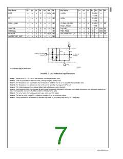
Note 8: Parasitics and or ESD protection circuitry are shown in the figure below for the LM87’s pins. The nominal breakdown voltage of the zener D3 is 6.5 V. Care
should be taken not to forward bias the parasitic diode, D1, present on pins: A0/NTEST_OUT, A1 and DACOut/NTEST_IN. Doing so by more than 50 mV may corrupt
a temperature or voltage measurement.
www.national.com
6

 NSC [ National Semiconductor ]