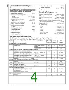
Absolute Maximum Ratings (Notes 1,
2)
Vapor Phase (60 seconds)
Infrared (15 seconds)
215 ˚C
235 ˚C
Storage Temperature
−65 ˚C to +150 ˚C
If Military/Aerospace specified devices are required,
please contact the National Semiconductor Sales Office/
Distributors for availability and specifications.
Operating Ratings(Notes 1, 2)
Operating Temperature Range
Positive Supply Voltage (V+)
Voltage on Any Input or Output Pin:
+12Vin
+6.0 V
T
≤ TA ≤ TMAX
MIN
LM87
−40 ˚C ≤ TA ≤ +125 ˚C
≤ TA ≤ TMAX
−0.3 V to +18 V
−0.3 V to
Specified Temperature Range
LM87
T
MIN
ADD/NTESTOUT,
−40 ˚C ≤ TA ≤ +125 ˚C
DACOut/NTEST_IN, AIN1, AIN2
All other pins
(V++ 0.3 V)
−0.3 V to +6 V
5 mA
Junction to Ambient Thermal Resistance (θJA(Note 5))
NS Package Number: MTC24B
Supply Voltage (V+)
95 ˚C/W
Input Current at any Pin (Note 4)
Package Input Current (Note 4)
Maximum Junction Temperature
(TJ max)
+2.8 V to +3.8 V
20 mA
V
Voltage Range:
IN
+12Vin
−0.05 V to +15 V
−0.05 V to +6.8 V
150 ˚C
+5Vin
ESD Susceptibility (Note 6)
Human Body Model
+3.3Vin
−0.05 V to +4.6 V
2500 V
150V
+2.5Vin
−0.05 V to +3.6 V
Machine Model
VID0 - VID4, Vccp
All other inputs
−0.05 V to +6.0 V
−0.05 V to (V++ 0.05 V)
Soldering Information
MTC Package (Note 7) :
DC Electrical Characteristics
The following specifications apply for +2.8 VDC ≤ V+ ≤ +3.8 VDC, Analog voltage inputs RS = 510 Ω, unless otherwise speci-
fied. Boldface limits apply for TA = T = TMIN to TMAX; all other limits TA = TJ = 25 ˚C.(Note 8)
J
Symbol
Parameter
Conditions
Typical
Limits
Units
(Note 9)
(Note 10)
(Limits)
POWER SUPPLY CHARACTERISTICS
I+
Supply Current
Normal Mode, Interface
Inactive
0.7
0.5
3
2.0
mA (max)
mA
Shutdown Mode
TEMPERATURE-TO-DIGITAL CONVERTER CHARACTERISTICS
Temperature Error using Internal Diode
˚C
Temperature Error using Remote Pentium
Diode Sensor (Note 11) and (Note 12)
Temperature Error using Remote 2N3904
Sensor (Note 11) and (Note 12)
0 ˚C ≤ TA ≤ +125 ˚C, Vcc
= 3.3 Vdc
3
4
˚C (max)
−40 ˚C ≤ TA ≤ +125 ˚C,
Vcc = 3.3 Vdc
˚C (max)
˚C (min)
Resolution
8 bits
1.0
LM87 ANALOG-TO-DIGITAL CONVERTER CHARACTERISTICS
Resolution
8
bits
% (max)
LSB (max)
sec
TUE
DNL
tC
Total Unadjusted Error
(Note 13)
(Note 14)
2
1
Differential Non-Linearity
Total Monitoring Cycle Time
0.28
130
ADC INPUT CHARACTERISTICS
Input Resistance (All analog inputs except
90
12
kΩ (min)
µA
AIN1 and AIN2)
AIN1 and AIN2 DC Input Current
DAC CHARACTERISTICS
Resolution
8
Bits
www.national.com
4

 NSC [ National Semiconductor ]