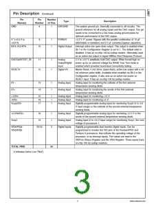
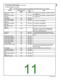
Pin Name
D1 D2 D3 R1 R2 R3 R4
Pin Name
D1 D2 D3 R1 R2 R3 R4
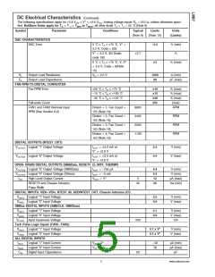
∞
∞
#
INT
x
x
x
x
x
x
x
x
x
0
0
0
100k 1M
+12Vin
x
x
x
x
x
x
R1+R2
≈130k
R1+R2
≈130k
R1+R2
≈130k
∞
∞
∞
∞
∞
∞
CI
1M
1M
+5Vin
FAN1–FAN2
+3.3Vin, +2.5Vin,
Vccp1, Vccp2
THERM
x
1M
∞
∞
∞
∞
∞
∞
∞
∞
∞
SMBCLK
SMBData
x
x
x
x
x
x
x
x
x
x
x
x
0
0
0
0
1M
1M
x
x
x
x
x
x
x
x
x
0
0
0
100k 1M
100k 1M
VID4–VID0
∞
#
RESET
100k 1M
DACOut/NTEST_IN
1M
∞
ADD/NTEST_OUT
1M
10099505
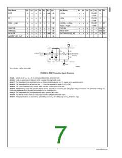
An x indicates that the diode exists.
FIGURE 2. ESD Protection Input Structure
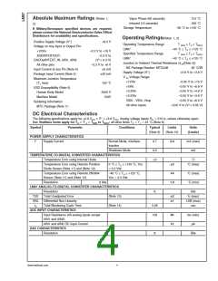
Note 9: Typicals are at T = T = 25 ˚C and represent most likely parametric norm.
J
A
Note 10: Limits are guaranteed to National’s AOQL (Average Outgoing Quality Level).
Note 11: The Temperature Error specification does not include an additional error of 1˚C, caused by the quantization error.
Note 12: The Temperature Error will vary less than 1˚C over the operating Vcc range of 2.8V to 3.8V.
Note 13: TUE (Total Unadjusted Error) includes Offset, Gain and Linearity errors of the ADC.
Note 14: Total Monitoring Cycle Time includes all diode checks, temperature conversions and analog input voltage conversions. Fan tachometer readings are
determined separately and do not affect the completion of the monitoring cycle.
Note 15: This is the lowest DAC code guaranteed to give a non-zero DAC output.
Note 16: The total fan count is based on 2 pulses per revolution of the fan tachometer output.
Note 17: Timing specifications are tested at the specified logic levels, V for a falling edge and V for a rising edge.
IL
IH
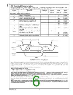
7
www.national.com

 NSC [ National Semiconductor ]