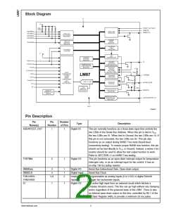
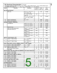
Block Diagram
10099501
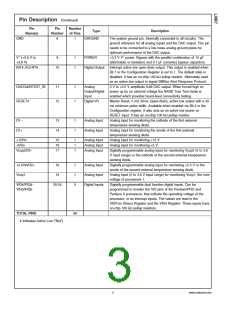
Pin Description
Pin
Name(s)
Pin
Number
Number
of Pins
1
Type
Description
ADD/NTEST_OUT
1
Digital I/0
This pin normally functions as a three-state input that controls the
two LSBs of the Serial Bus Address. When this pin is tied to VCC
the two LSBs are 01. When tied to Ground, the two LSBs are 10. If
this pin is not connected, the two LSBs are 00. This pin also
functions as an output during NAND Tree tests (board-level
connectivity testing). To ensure proper NAND tree function, this pin
should not be tied directly to VCC or Ground. Instead, a series 5 kΩ
resistor should be used to allow the test output function to work.
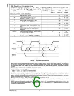
Refer to SECTION 11 on NAND Tree testing.
#
THERM
2
1
Digital I/O
This pin functions as an open-drain interrupt output for temperature
interrupts only, or as an interrupt input for fan control. It has an
on-chip 100 kΩ pullup resistor.
SMBData
SMBCLK
FAN1/AIN1-
FAN2/AIN2
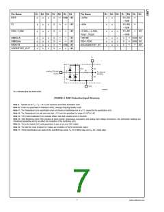
CI
3
4
1
1
2
Digital I/O
Digital Input
Analog/Digital
Inputs
Serial Bus bidirectional Data. Open-drain output.
Serial Bus Clock.
5-6
Programmable as analog inputs (0 to 2.5V) or digital Schmitt
Trigger fan tachometer inputs.
7
1
Digital I/O
An active high input from an external circuit which latches a
Chassis Intrusion event. This line can go high without any clamping
action regardless of the powered state of the LM87. There is also
an internal open-drain output on this line, controlled by Bit 7 of the
CI Clear Register (46h), to provide a minimum 20 ms pulse.
www.national.com
2

 NSC [ National Semiconductor ]