5.0 LAYOUT AND GROUNDING
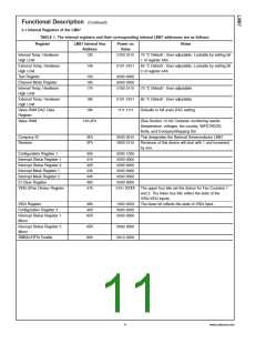
Functional Description (Continued)
A separate, low-impedance ground plane for analog ground,
which provides a ground point for the GND pin, voltage
dividers and other analog components, will provide best
performance, but is not mandatory. Analog components such
as voltage dividers should be located physically as close as
possible to the LM87.
The power supply bypass, the parallel combination of 10 µF
(electrolytic or tantalum) and 0.1 µF (ceramic) bypass ca-
pacitors connected between pin 9 and ground, should also
be located as close as possible to the LM87.
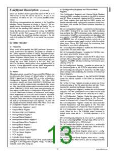
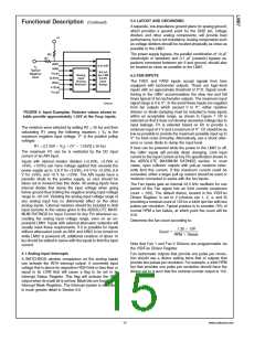
6.0 FAN INPUTS
The FAN1 and FAN2 inputs accept signals from fans
equipped with tachometer outputs. These are logic-level
inputs with an approximate threshold of V+/2. Signal condi-
tioning in the LM87 accommodates the slow rise and fall
times typical of fan tachometer outputs. The maximum input
signal range is 0 to V+. In the event these inputs are supplied
from fan outputs which exceed 0 to V+, either resistive
division or diode clamping must be included to keep inputs
within an acceptable range, as shown in Figure 7. R2 is
selected so that it does not develop excessive voltage due to
input leakage. R1 is selected based on R2 to provide a
minimum input of 2 V and a maximum of V+. R1 should be as
low as possible to provide the maximum possible input up to
V+ for best noise immunity. Alternatively, use a shunt refer-
ence or zener diode to clamp the input level.
10099530
FIGURE 6. Input Examples. Resistor values shown in
table provide approximately 1.25V at the Vccp inputs.
The resistors were selected by setting R2 = 20 kΩ and then
calculating R1 using the following equation, ( VS is the
maximum negative input voltage, V+ is the positive pullup
voltage):
R1 = [(1.25V − VS) ÷ (V+ − 1.25V)] x 20 kΩ
The maximum R1 can be is restricted by the DC input
current of an AIN input.
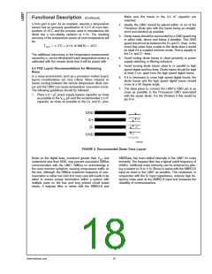
If fans can be powered while the power to the LM87 is off,
the LM87 inputs will provide diode clamping. Limit input
current to the Input Current at Any Pin specification shown in
the ABSOLUTE MAXIMUM RATINGS section. In most
cases, open collector outputs with pull-up resistors inher-
ently limit this current. If this maximum current could be
exceeded, either a larger pull up resistor should be used or
resistors connected in series with the fan inputs.
Inputs with internal resistor dividers (+2.5Vin, +3.3Vin or
+5Vin, +12Vin) can have voltage applied that exceeds the
power supply up to: 3.6 V for +2.5Vin, 4.6 V for +3.3Vin, 6.8
V for +5Vin, and 15 V for +12Vin. The AIN inputs have a
parasitic diode to the positive supply, so care should be
taken not to forward bias this diode. All analog inputs have
internal diodes that clamp the input voltage when going
below ground thus limiting the negative analog input voltage
range to −50 mV. Violating the analog input voltage range of
any analog input has no detrimental effect on the other
analog inputs. External resistors should be included to limit
input currents to the values given in the ABSOLUTE MAXI-
MUM RATINGS for Input Current At Any Pin whenever ex-
ceeding the analog input voltage range, even on an un-
powered LM87. Inputs with external attenuator networks will
usually meet these requirements. If it is possible for inputs
without attenuators (such as AIN1 and AIN2) to be turned on
while LM87 is powered off, additional resistors of about 10
kΩ should be added in series with the inputs to limit the input
current.
The Fan Inputs gate an internal 22.5 kHz oscillator for one
period of the Fan signal into an 8-bit counter (maximum
count = 255). The default divisor, located in the VID/Fan
Divisor Register, is set to 2 (choices are 1, 2, 4, and 8)
providing a nominal count of 153 for a 4400 rpm fan with two
pulses per revolution. Typical practice is to consider 70% of
normal RPM a fan failure, at which point the count will be
219.
Determine the fan count according to:
Note that Fan 1 and Fan 2 Divisors are programmable via
the VID/Fan Divisor Register.
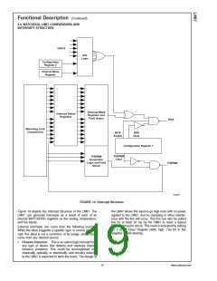
4.1 Analog Input Interrupts
Fan tachometer outputs that provide one pulse per revolu-
tion should use a divisor setting twice that of outputs that
provide two pulses per revolution. For example, a 4400 RPM
fan that provides one pulse per revolution should have the
divisor set to 4 such that the nominal counter output is 153.
A WATCHDOG window comparison on the analog inputs
#
can activate the INT interrupt output. A converted input
voltage that is above its respective HIGH limit or less than or
equal to its LOW limit will cause a flag to be set in its
#
Interrupt Status Register. This flag will activate the INT
output when its mask bit is set low. Mask bits are found in the
Interrupt Mask Registers. The Interrupt system is described
in much greater detail in Section 9.0.
15
www.national.com

 NSC [ National Semiconductor ]