than once every 0.6 seconds can also prevent complete
updates of Interrupt Status Registers and Interrupt Output’s.
Functional Description (Continued)
Bit 2 of the Channel Mode Register, when set to 0, config-
ures pins 18 and 19 as +2.5V and VCCP2 voltage inputs.
When set to 1, pins 18 and 19 are configured as a second
remote temperature sensing channel.
A typical sequence of events upon power on of the LM87
would consist of:
1. Set WATCHDOG Limits
2. Set Interrupt Masks
Bit 3 of the Channel Mode Register, when set to 0, sets the
nominal voltage for internal VCC measurement to 3.3V.
When set to 1, the nominal VCC range is 5V.
3. Start the LM87 monitoring process
4.0 ANALOG INPUTS
Bit 4 of the Channel Mode Register, when set to 1, enables
pin 24 as an active low (IRQ0) interrupt input. When set to 0,
this input is disabled as an IRQ interrupt.
All analog input voltages are digitized to 8-bits of resolution.
For safety purposes, and to provide maximum accuracy, a
510 Ω resistor should be placed in series with all analog
voltage inputs. The resistors will limit the possible current
drawn from the power supplies in the event that circuit board
traces are bridged, or accidentally shorted during test. All
analog inputs, except for AIN1 and AIN2, include internal
resistor attenuators. The theoretical LSB size, theoretical
voltage input required for an ADC reading of 192 (3/4 scale)
and 255 (full scale) for each analog input is detailed in the
table below:
Bit 5 of the Channel Mode Register, when set to 1, enables
pin 23 as an active low (IRQ1) interrupt input. When set to 0,
this input is disabled as an IRQ interrupt.
Bit 6 of the Channel Mode Register, when set to 1, enables
pin 22 as an active low (IRQ2) interrupt input. When set to 0,
this input is disabled as an IRQ interrupt.
Bit 7 of the Channel Mode Register, when set to 1, config-
ures pins 20 to 24 as interrupt inputs. When set to 0, pins 20
to 24 are configured as processor voltage ID pins.
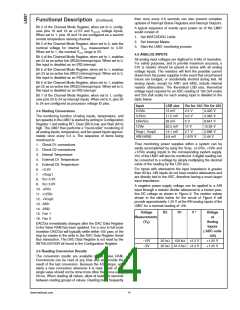
Input
LSB size
13 mV
Vin for 192 Vin for 255
2.5Vin
2.5 V
3.3 V
5 V
3.320 V
4.383 V
6.641 V
15.93 V
3.586 V
2.49 V
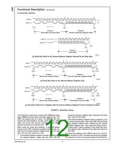
3.4 Starting Conversions
The monitoring function (Analog inputs, temperature, and
fan speeds) in the LM87 is started by writing to Configuration
Register 1 and setting INT_Clear (Bit 3) low, and Start (bit 0)
high. The LM87 then performs a “round-robin” monitoring of
all analog inputs, temperature, and fan speed inputs approxi-
mately once every 0.3 s. The sequence of items being
monitored is:
3.3Vcc
17.2 mV
26 mV
5Vin/Vcc
12Vin
62.5 mV
14.1 mV
9.8 mV
12 V
Vccp1, Vccp2
AIN1/AIN2
2.7 V
1.875 V
Thus monitoring power supplies within a system can be
easily accomplished by tying the Vccp, +2.5Vin, +5Vin and
+12Vin analog inputs to the corresponding system supply.
Vcc of the LM87 will also be monitored. A digital reading can
be converted to a voltage by simply multiplying the decimal
value of the reading by the LSB size.
1. Check D1 connections
2. Check D2 connections
3. Internal Temperature
4. External D1 Temperature
5. External D2 Temperature
6. +2.5V
For inputs with attenuators the input impedance is greater
than 90 kΩ. AIN inputs do not have resistor attenuators and
are directly tied to the ADC, therefore having a much larger
input impedance.
7. +Vccp1
8. Vcc 3.3V
9. Vcc 5.0V
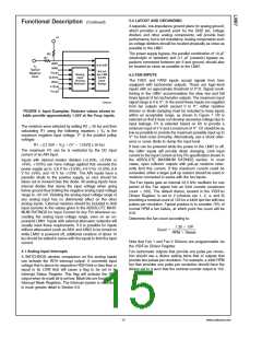
A negative power supply voltage can be applied to a AIN
input through a resistor divider referenced to a known posi-
tive DC voltage as shown in Figure 6. The resistor values
shown in the table below for the circuit of Figure 6 will
provide approximately 1.25 V at the AIN analog inputs of the
LM87 for a nominal reading of 128.
10. +5Vin
11. +12Vin
12. +Vccp2
13. AIN1
14. AIN2
Voltage
Measurements
(VS)
R2
R1
V +
Voltage
at
Analog
Inputs
( ADC code
128)
15. Fan 1
16. Fan 2
DACOut immediately changes after the DAC Data Register
in the Value RAM has been updated. For a zero to full scale
transition DACOut will typically settle within 100 µsec of the
stop by master in the write to the DAC Data Register Serial
Bus transaction. The DAC Data Register is not reset by the
INITIALIZATION bit found in the Configuration Register.
−12V
−5V
20 kΩ 130 kΩ +3.3 V
20 kΩ 61.0 kΩ +3.3 V
+1.25 V
+1.25 V
3.5 Reading Conversion Results
The conversion results are available in the Value RAM.
Conversions can be read at any time and will provide the
result of the last conversion. Because the ADC stops, and
starts a new conversion whenever it is read, reads of any
single value should not be done more often than once every
56 ms. When reading all values, allow at least 0.6 seconds
between reading groups of values. Reading more frequently
www.national.com
14

 NSC [ National Semiconductor ]