3.3 Configuration Registers and Channel Mode
Register
Functional Description (Continued)
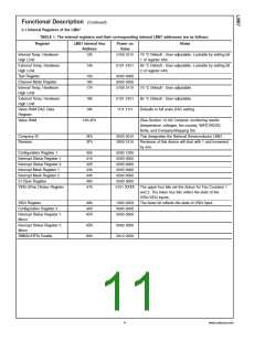
power up. If ADD is tied to ground the value for XY is 10. If
ADD is tied to Vcc XY will be set to 01. If ADD is not
connected, XY will be 00. XY = 11 is not a possible combi-
nation.
The Configuration Registers and Channel Mode Register
control the LM87 operation. At power on, the ADC is stopped
#
and INT_Clear is asserted, clearing the INT hardwire out-
put. These registers start and stop the LM87, enable and
disable interrupt output, configure the operation of dual func-
tion inputs, and provide the Reset functions described in
Section 3.2.
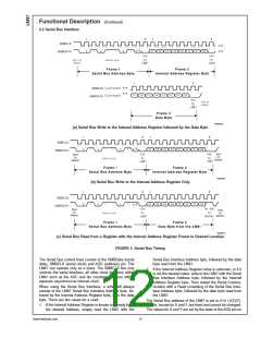
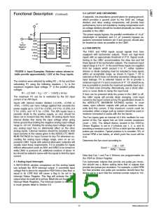
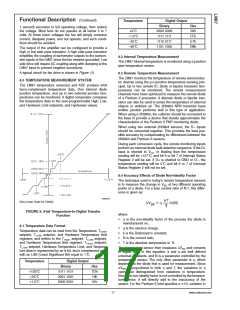
All of these communications are depicted in the Serial Bus
Interface Timing Diagrams as shown in Figure 5. The ex-
ample shown corresponds to the ADD pin tied to Vcc, so
XY=01 and the resulting LM87 address is 0101101.
Bit 0 of Configuration Register 1 controls the monitoring loop
of the LM87. Setting Bit 0 low stops the LM87 monitoring
loop and puts the LM87 in shutdown mode, reducing power
consumption. Serial Bus communication can take place with
any register in the LM87 although activity on the SMBData
and SMBCLK lines will increase shutdown current, up to as
much as maximum rated supply current, while the activity
takes place. Taking Bit 0 high starts the monitoring loop,
described in more detail subsequently.
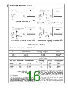
Serial Bus Timeout can be initiated by holding the SMBCLK
line low for greater than tTIMEOUT (35 ms max). Serial Bus
Timeout resets the serial bus interface circuitry to the idle
state and readies the LM87 for a new serial bus communi-
cation.
3.0 USING THE LM87
3.1 Power On
#
Bit 1 of Configuration Register 1 enables the INT Interrupt
When power is first applied, the LM87 performs a “power on
reset” on several of its registers. The power on condition of
the LM87’s registers is shown in Table 1. The internal regis-
ters and their corresponding internal LM87 addresses are as
follows: Registers whose power on values are not shown
have power on conditions that are indeterminate (this in-
cludes the value RAM ,exclusive of the DAC data, and
WATCHDOG limits). When power is first applied the ADC is
inactive. In most applications, the first action after power on
is to write WATCHDOG limits into the Value RAM.
output when this bit is taken high.
#
Bit 2 of Configuration Register 1 enables the THERM Inter-
rupt output when this bit is taken high.
Bit 3 of Configuration Register 1 clears the INT# output when
set high, without affecting the contents of the Interrupt Status
Registers. The LM87 will stop monitoring. It will resume upon
clearing of this bit.
Bit 4 of Configuration Register 1 provides an active low 20
ms (minimum) pulse at the RESET output when set high.
#
Bit 6 of Configuration Register 1 clears the THERM# output
when set high, without affecting the contents of the Interrupt
Status Registers.
3.2 Resets
All register values, except the Programmed DAC Output can
be returned to their "power on" default values by taking the
Bit 7 of Configuration Register 1 (the INITIALIZATION bit)
resets the internal registers of the LM87 as described in
Section 3.2.
#
RESET input low for at least TBD ns or by performing a
Configuration Register INITIALIZATION. The Value RAM
conversion results, and Value RAM WATCHDOG limits are
not Reset and will be indeterminate immediately after power
on. If the Value RAM contains valid conversion results and/or
Value RAM WATCHDOG limits have been previously set,
they will not be affected by a Configuration Register INITIAL-
IZATION. The Power On Reset, RESET# input, and Configu-
ration Register INITIALIZATION, clear or initialize the follow-
ing registers (the initialized values are shown on Table I).
Power On Reset also sets the Programmed DAC Output to
full scale (FFh) Hardware High Limit registers 13h, and 14h
will only be returned to default values if the "Write Once" bits
in Configuration Register 2 have not been set:
Bit 7 of the CI_Clear Register provides an active low 20 ms
#
(minimum) pulse at the CI output pin when set high. This is
intended for resetting the Chassis Intrusion circuitry.
#
Bit 0 of Configuration Register 2 enables the INT Interrupt
output for THERM# events when set low. When this bit is set
high, THERM# error events will not affect the INT# output.
Bit 1 of Configuration Register 2 locks the value set in the
Internal Temperature high limit register at 13h. The value
cannot be changed until a Power On Reset is performed.
Bit 2 of Configuration Register 2 locks the value set in the
External Temperature high limit register at 14h. The value
cannot be changed until a Power On Reset is performed.
•
•
•
•
•
•
•
•
•
•
•
•
•
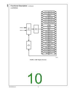
Configuration Registers 1 and 2
Channel Mode Register
Bit 3 of Configuration Register 2 sets the THERM# output
mode. When set to 0, the THERM# output functions in
default mode, when set to 1, THERM# operates in ACPI
mode.
Hardware High Limit Registers
Interrupt Status Register 1
Interrupt Status Register 2
Interrupt Status Mirror Register 1
Interrupt Status Mirror Register 2
Interrupt Mask Register 1
Interrupt Mask Register 2
Chassis Intrusion Clear Register
VID/Fan Divisor Register
VID4 Register
Bit 6 of Configuration Register 2, when set to 1, enables pin
21 as an active high (IRQ3) interrupt input. When set to 0,
this input is disabled as an IRQ interrupt.
Bit 7 of Configuration Register 2, when set to 1, enables pin
20 as an active high (IRQ4) interrupt input. When set to 0,
this input is disabled as an IRQ interrupt.
Bit 0 of the Channel Mode Register, when set to 1, config-
ures pin 5 as AIN1. When set to 0, pin 5 is configured as the
FAN1 input.
Extended Mode Register
Bit 1 of the Channel Mode Register, when set to 1, config-
ures pin 6 as AIN2. When set to 0, pin 6 is configured as the
FAN2 input.
Configuration Register INITIALIZATION is accomplished by
setting Bit 7 of Configuration Register 1 high. This bit auto-
matically clears after being set.
13
www.national.com

 NSC [ National Semiconductor ]