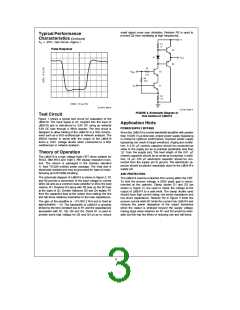
Application Hints (Continued)
TL/H/11442–8
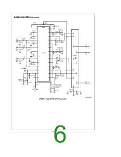
FIGURE 3. Typical Application Circuit (One Channel)
IMPROVING RISE AND FALL TIMES
Table I. LM2419 Output Overshoot
vs Capacitive Loading for a Typical Device
Because of an emitter follower output stage, the rise and fall
times of the LM2419 are relatively unaffected by capacitive
loading. However, the series resistors R1 and R2 (see Fig-
ure 3 ) will reduce the rise and fall times when driving the
CRT’s cathode which appears as a capacitive load. The ca-
pacitance at the cathode typically ranges from 8 pF to
12 pF.
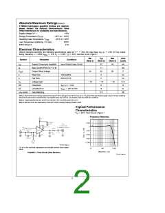
Input Signal
t /t
C
L
r
f
5 pF
4%
4%
8 pF
6%
5%
11 pF
7%
15 pF
8%
1.2 ns
7 ns
6%
7%
To improve the rise and fall times at the cathode, a small
inductor is often used in series with the output of the amplifi-
er. The inductor L1 in Figure 3 peaks the amplifier’s fre-
quency response at the cathode, thus improving rise and fall
times. The inductor value is empirically determined and is
dependent on the load. An inductor value of 0.1 mH is a
good starting value. Note that peaking the amplifier’s fre-
quency response will increase the overshoot.
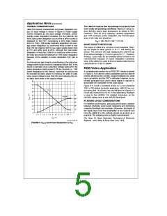
GAIN VS OUTPUT DC LEVEL
Figure 4 shows LM2419’s gain versus output DC level. A
100 mV AC signal is applied at the LM2419’s input and
PP
the input signal’s DC level is swept. As can be seen from
Figure 4, the amplifier’s gain is constant at approximately
e
15.4 (V
OUT
1.54 V ) for output DC level between 35V
PP
and 65V. Thus the amplifier’s output response is linear for
output voltage between 35V and 65V. If the output voltage
is less than 35V or more than 70V, the amplifier’s output
response becomes non-linear (note the change in gain, Fig-
ure 4 ). For optimum performance, it is recommended that
LM2419’s output low voltage be at 25V or above. For a
REDUCING OVERSHOOT
LM2419’s overshoot is a function of both the input signal
rise and fall times and the capacitive loading. The overshoot
is increased by either more capacitive loading or faster rise
and fall times of the input signal.
50 V swing, the output high voltage is 75V. With an output
PP
Table I shows the overshoot for a typical device with differ-
ent capacitive loads and different input signal rise and fall
times. As can be observed from Table I, overshoot is large
for large capacitive loads and faster input signal rise and fall
times. In an actual application, the LM2419 is driven from a
preamplifier with rise and fall times of 3 ns to 7 ns. When
driven from LM1203 preamplifier (see application circuit,
Figure 6 ) the overshoot is 10% with 12 pF capacitive load.
The overshoot can be reduced by including a resistor in
series with LM2419’s output as in Figure 3. Larger value
resistors for R1 and R2 would reduce overshoot but this
also increases the rise and fall times at the output. Frequen-
cy peaking using an inductor in series with the output may
restore the bandwidth.
signal swing from 25V to 75V, LM2419’s linearity error is
measured at 8%.
TL/H/11442–9
e
FIGURE 4. Gain vs V
OUT
(DC), V
IN
100 mV
PP
4

 NSC [ National Semiconductor ]