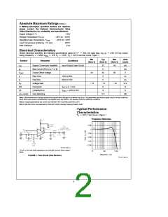
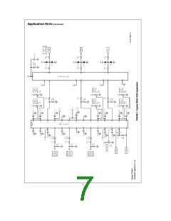
small signal cross over distortion. Resistor R3 is used to
prevent Q2 from oscillating at high frequencies.
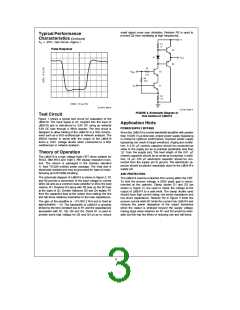
Typical Performance
Characteristics (Continued)
e
T
A
25 C, Test CircuitÐFigure 1
§
Pulse Response
TL/H/11442–5
TL/H/11442–7
FIGURE 2. Schematic Diagram of
One Section of LM2419
Test Circuit
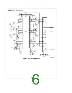
Figure 1 shows a typical test circuit for evaluation of the
LM2419. The input signal is AC coupled into the input of
LM2419 and is referenced to 3.9V DC using an external
3.9V DC bias through a 390X resistor. The test circuit is
designed to allow testing of the LM2419 in a 50X environ-
ment such as a 50X oscilloscope or network analyzer. The
4950X resistor in series with the output of the LM2419
forms a 100:1 voltage divider when connected to a 50X
oscilloscope or network analyzer.
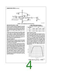
Application Hints
POWER SUPPLY BYPASS
Since the LM2419 is a wide-bandwidth amplifier with greater
than 10,000 V/ms slew rate, proper power supply bypassing
is critical for optimum performance. Improper power supply
bypassing can result in large overshoot, ringing and oscilla-
tion. A 0.01 mF ceramic capacitor should be connected as
close to the supply pin as is practical (preferably less than
(/4 from the supply pin). The lead length of the 0.01 mF
×
Theory of Operation
ceramic capacitor should be as small as is practical. In addi-
tion, 10 mF–100 mF electrolytic capacitor should be con-
nected from the supply pin to ground. The electrolytic ca-
pacitor should be placed reasonably close to the LM2419’s
supply pin.
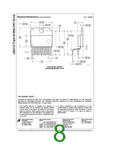
The LM2419 is a high voltage triple CRT driver suitable for
SVGA, IBM 8514 and 1024 x 768 display resolution moni-
tors. The device is packaged in the industry standard
11 lead TO-220 molded power package. The heat sink is
electrically isolated and may be grounded for ease of manu-
facturing and RFl/EMl shielding.
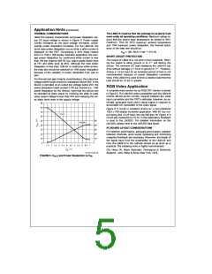
ARC PROTECTION
The schematic diagram of LM2419 is shown in Figure 2. Q1
and R2 provide a conversion of the input voltage to current
while Q2 acts as a common base amplifier to drive the load
resistor, R1. Resistor R4 along with R2 sets up the DC bias
at the base of Q1. Emitter followers Q3 and Q4 isolate R1
from the capacitive load at the output, thus making the rise
and fall times relatively insensitive to the load capacitance.
The LM2419 must be protected from arcing within the CRT.
To limit the arcover voltage, a 200V spark gap is recom-
mended at the cathode. Clamp diodes D1 and D2 (as
shown in Figure 3 ) are used to clamp the voltage at the
output of LM2419 to a safe level. The clamp diodes used
should have high current rating, low series impedance and
low shunt capacitance. Resistor R2 in Figure 3 limits the
arcover current while R1 limits the current into LM2419 and
reduces the power dissipation of the output transistors
when the output is stressed beyond the supply voltage.
Having large value resistors for R1 and R2 would be desir-
able but this has the effect of reducing rise and fall times.
b
The gain of the amplifier is R1/(R2 R4) and is fixed at
approximately 15. The bandwidth of LM2419 is primarily
ll
b
limited by the time constant due to R1 and the capacitances
associated with D1, Q2, Q3 and Q4. Diode D1 is used to
provide some bias voltage for Q3 and Q4 so as to reduce
3

 NSC [ National Semiconductor ]