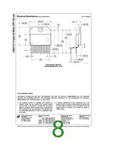
Absolute Maximum Ratings (Note 1)
If Military/Aerospace specified devices are required,
please contact the National Semiconductor Sales
Office/Distributors for availability and specifications.
Supply Voltage (Va
)
85V
25 C to 100 C
a
b
a
Storage Temperature (T
)
§
20 C to 90 C
§
STG
b
a
Operating Case Temperature, T
§
§
Case
k
Lead Temperature (soldering 10 sec.)
ESD Tolerance
300 C
§
2 kV
Electrical Characteristics
Unless otherwise specified, the following specifications apply for Va
80V, DC input bias, V
e
25 C; see test circuit, Figure 1.
e
3.9V; 50 V output
PP
IN DC
e
e
e
e
12 pF; T
A
swing; frequency
1 MHz; V
12V; C
§
Bias
L
Min
Typ
Max
Units
Symbol
Parameter
Conditions
(Note 3)
(Note 2)
(Note 3)
(Limit)
I
I
Supply Current (per Amplifier)
Bias Current (Pins 2 or 7 or 9)
Output Offset Voltage
Rise Time
Input/Output Open Circuit
27
11
50
5
40
60
mA
mA
V
CC
B
V
40
OUT
t
t
10% to 90%
90% to 10%
ns
r
f
Fall Time
5
ns
b
b
b
18
A
Voltage Gain
13
15
V/V
%
V
k
: t , t
r f
OS
LE
Overshoot
V
V
2 ns
8
IN
e
Linearlty Error
25V to 75V
8
%
OUT
DA match
V
Gain Matching
0.3
dB
Note 1: Absolute Maximum Ratings indicate limits beyond which damage to the device may occur. The guaranteed specifications apply only for the test conditions
listed. Some performance characteristics may degrade when the device is not operated under the listed test conditions.
Note 2: Typical specifications are at 25 C and represent the most likely parametric norm.
§
Note 3: Min/Max limits are guaranteed to National’s AOQL (Average Outgoing Quality Level).
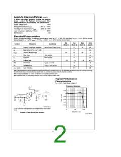
Typical Performance
Characteristics
e
T
A
25 C, Test CircuitÐFigure 1
§
Frequency Response
TL/H/11442–3
*12 pF is the total load capacitance and includes the test fixture capaci-
tance.
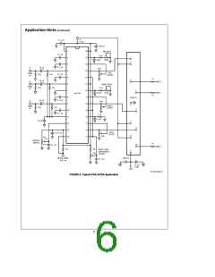
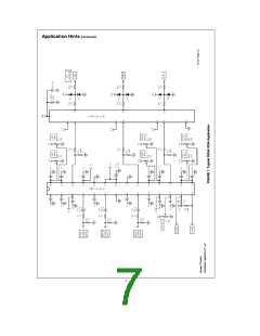
FIGURE 1. Test Circuit (One Section)
TL/H/11442–4
2

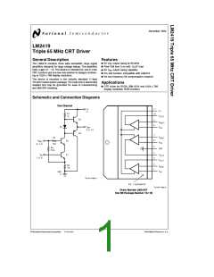
 NSC [ National Semiconductor ]