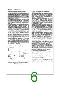
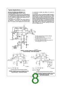
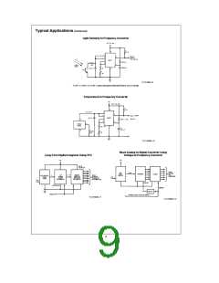
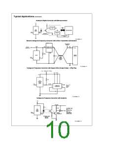
Typical Applications (Continued)
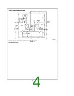
PRINCIPLES OF OPERATION OF A SIMPLIFIED
VOLTAGE-TO-FREQUENCY CONVERTER
DETAIL OF OPERATION, FUNCTIONAL BLOCK
DIAGRAM (FIGURE 1a)
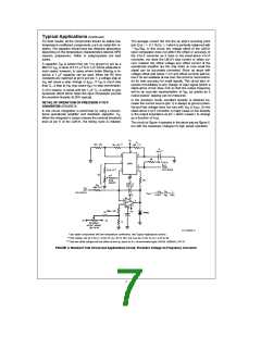
The LM131 is a monolithic circuit designed for accuracy and
versatile operation when applied as a voltage-to-frequency
(V-to-F) converter or as a frequency-to-voltage (F-to-V) con-
verter. A simplified block diagram of the LM131 is shown in
Figure 2 and consists of a switched current source, input
comparator, and 1-shot timer.
The block diagram shows a band gap reference which pro-
vides a stable 1.9 V output. This 1.9 V is well regulated
DC DC
over a V range of 3.9V to 40V. It also has a flat, low tem-
S
perature coefficient, and typically changes less than (/2%
over a 100 C temperature change.
§
The current pump circuit forces the voltage at pin 2 to be at
e
1.90V/R to flow. For
S
The operation of these blocks is best understood by going
through the operating cycle of the basic V-to-F converter,
Figure 2, which consists of the simplified block diagram of
the LM131 and the various resistors and capacitors con-
nected to it.
1.9V, and causes
e
a
current
i
e
R
14k, i 135 mA. The precision current reflector pro-
s
vides a current equal to i to the current switch. The current
switch switches the current to pin 1 or to ground depending
on the state of the R flip-flop.
S
The voltage comparator compares a positive input voltage,
V1, at pin 7 to the voltage, V , at pin 6. If V1 is greater, the
x
comparator will trigger the 1-shot timer. The output of the
timer will turn ON both the frequency output transistor and
The timing function consists of an R flip-flop, and a timer
S
comparator connected to the external R C network. When
t t
the input comparator detects a voltage at pin 7 higher than
pin 6, it sets the R flip-flop which turns ON the current
S
switch and the output driver transistor. When the voltage at
e
the switched current source for a period t 1.1 R C . During
this period, the current i will flow out of the switched current
t
t
pin 5 rises to )/3 V , the timer comparator causes the R
CC
S
e
c
t, into
the capacitor, C . This will normally charge V up to a higher
source and provide a fixed amount of charge, Q
i
flip-flop to reset. The reset transistor is then turned ON and
the current switch is turned OFF.
L
x
level than V1. At the end of the timing period, the current i
will turn OFF, and the timer will reset itself.
However, if the input comparator still detects pin 7 higher
than pin 6 when pin 5 crosses )/3 V , the flip-flop will not
CC
Now there is no current flowing from pin 1, and the capaci-
tor C will be gradually discharged by R until V falls to the
level of V1. Then the comparator will trigger the timer and
start another cycle.
be reset, and the current at pin 1 will continue to flow, in its
attempt to make the voltage at pin 6 higher than pin 7. This
condition will usually apply under start-up conditions or in
the case of an overload voltage at signal input. It should be
noted that during this sort of overload, the output frequency
will be 0; as soon as the signal is restored to the working
range, the output frequency will be resumed.
L
L
x
e
c
c
t
The current flowing into C is exactly I
c
i
(1.1 R C )
L
AVE
f, and the current flowing out of C is exactly V /R
L
t
j
L
x
V
/R . If V is doubled, the frequency will double to main-
IN IN
L
tain this balance. Even a simple V-to-F converter can pro-
vide a frequency precisely proportional to its input voltage
over a wide range of frequencies.
The output driver transistor acts to saturate pin 3 with an
ON resistance of about 50X. In case of overvoltage, the
output current is actively limited to less than 50 mA.
The voltage at pin 2 is regulated at 1.90 V for all values of
DC
i between 10 mA to 500 mA. It can be used as a voltage
reference for other components, but care must be taken to
ensure that current is not taken from it which could reduce
the accuracy of the converter.
PRINCIPLES OF OPERATION OF BASIC VOLTAGE-
TO-FREQUENCY CONVERTER (FIGURE 1)
The simple stand-alone V-to-F converter shown in Figure 1
includes all the basic circuitry of Figure 2 plus a few compo-
nents for improved performance.
e
g
100 kX 10%, has been added in the path
A resistor, R
IN
b
to pin 7, so that the bias current at pin 7 ( 80 nA typical)
will cancel the effect of the bias current at pin 6 and help
provide minimum frequency offset.
The resistance R at pin 2 is made up of a 12 kX fixed
S
resistor plus a 5 kX (cermet, preferably) gain adjust rheo-
stat. The function of this adjustment is to trim out the gain
TL/H/5680–4
FIGURE 2. Simplified Block Diagram of Stand-Alone
Voltage-to-Frequency Converter Showing LM131 and
External Components
tolerance of the LM131, and the tolerance of R , R and C .
t
t
L
6

 NSC [ National Semiconductor ]