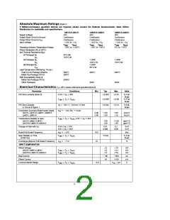
Absolute Maximum Ratings (Note 1)
If Military/Aerospace specified devices are required, please contact the National Semiconductor Sales Office/
Distributors for availability and specifications.
LM131A/LM131
40V
LM231A/LM231
40V
LM331A/LM331
40V
Supply Voltage
Output Short Circuit to Ground
Continuous
Continuous
Continuous
Continuous
Continuous
Continuous
Output Short Circuit to V
Input Voltage
CC
b
a
b
a
b
a
0.2V to V
S
0.2V to
V
S
0.2V to
V
S
T
b
T
T
b
T
T
T
MAX
0 C to 70 C
MIN
MAX
MIN
MAX
MIN
a
55 C to 125 C
a
25 C to 85 C
a
Operating Ambient Temperature Range
§
§
§
§
§
§
Power Dissipation (P at 25 C)
§
D
and Thermal Resistance (i
(H Package) P
)
jA
670 mW
D
i
(N Package) P
150 C/W
§
jA
1.25W
1.25W
D
i
(M Package)P
100 C/W
§
1.25W
100 C/W
§
jA
D
i
85 C/W
§
JA
Lead Temperature (Soldering, 10 sec.)
Dual-In-Line Package (Plastic)
Metal Can Package (TO-5)
ESD Susceptibility (Note 4)
Metal Can Package (TO-5)
Other Packages
260 C
§
260 C
§
260 C
§
260 C
§
2000V
500V
500V
e
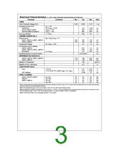
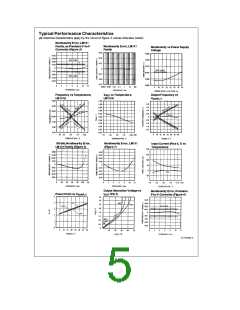
Electrical Characteristics T 25 C unless otherwise specified (Note 2)
§
A
Parameter
Conditions
Min
Typ
Max
Units
s
s
s
g
g
g
VFC Non-Linearity (Note 3)
4.5V
V
20V
0.003
0.006
0.01
0.02
% Full-
Scale
% Full-
Scale
S
s
g
g
T
T
T
MAX
MIN
A
e
e
10 Hz to 11 kHz
g
VFC Non-Linearity
In Circuit ofFigure 1
V
V
15V, f
0.024
0.14
%Full-
Scale
S
e b
e
14 kX
Conversion Accuracy Scale Factor (Gain)
LM131, LM131A, LM231, LM231A
LM331, LM331A
10V, R
IN
S
0.95
0.90
1.00
1.00
1.05
1.10
kHz/V
kHz/V
s
s
s
s
V 20V
S
Temperature Stability of Gain
LM131/LM231/LM331
LM131A/LM231A/LM331A
T
MIN
T
A
T , 4.5V
MAX
g
g
g
150
30
20
ppm/ C
§
g
50
0.1
0.06
ppm/ C
§
s
s
s
s
Change of Gain with V
4.5V
10V
V
V
10V
40V
0.01
0.006
%/V
%/V
S
S
S
e b
s
Rated Full-Scale Frequency
V
10V
10.0
10
kHz
IN
s
g
Gain Stability vs Time
(1000 Hrs)
T
MIN
T
A
T
MAX
0.02
% Full-
Scale
e b
Overrange (Beyond Full-Scale) Frequency
V
IN
11V
%
INPUT COMPARATOR
g
g
g
g
g
g
Offset Voltage
3
4
3
10
14
10
mV
mV
mV
s
s
s
LM131/LM231/LM331
LM131A/LM231A/LM331A
T
T
T
T
T
T
MIN
MIN
A
A
MAX
MAX
s
s
b
b
g
Bias Current
80
300
100
nA
nA
V
g
Offset Current
8
s
b
b
2.0
Common-Mode Range
T
MIN
T
A
T
MAX
0.2
V
CC
2

 NSC [ National Semiconductor ]