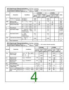
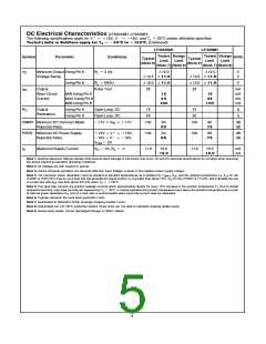
DC Electrical Characteristics (LF400AMHꢂ LF400MH)
b
The following specifications apply for Va
Tested Limits in Boldface apply for T
15Vꢂ V
e b
e a
e b
e
15Vꢂ and T 25 C unless otherwise specifiedꢁ
J
ꢀ
a
55 C to 125 Cꢀ (Continued)
ꢀ
ꢀ
J
LF400AMH
LF400MH
Tested Design
Tested Design
Symbol
Parameter
Conditions
Units
Typical
(Note 6)
Typical
(Note 6)
Limit
Limit
Limit
Limit
(Note 7) (Note 8)
(Note 7) (Note 8)
e
e
g
g
12ꢁ0
V
Minimum Output Using Pin 6
Voltage Swing
R
R
2 kX
12ꢁ0
V
V
O
L
g
12ꢁ5
g
12ꢁ0
25
g
g
12ꢁ5
g
12ꢁ0
25
g
11ꢀ5
11ꢀ5
g
g
Using Pin 8
Output
600X
11ꢀ0
11ꢀ0
V
L
I
Pulse Test
mA
mA
mA
mA
SC
Short Circuit
Current
MIN Using Pin 6
15
45
15
45
MAX Using Pin 6
MIN Using Pin 8
100
100
R
O
Output
Using Pin 6
Using Pin 8
Open Loopꢂ DC
Open Loopꢂ DC
75
50
75
50
X
X
Resistance
s
s
b
a
a
CMRR Minimum DC Common Mode
Rejection Ratio
11V
V
11V
100
90
100
80
dB
dB
IN
80
75
a
s
s
s
s
a
b
PSRR Minimum DC Power Supply
Rejection Ratio
10V
15V
V
V
15Vꢂ
10Vꢂ
100
90
100
80
dB
dB
b
b
85
75
e
V
0V
CM
e
e %
0Vꢂ R
L
I
Maximum Supply Current
V
O
11ꢁ0
13ꢁ0
11ꢁ0
13ꢁ0
mA
mA
S
13ꢀ0
15ꢀ0
Note 1ꢁ Absolute Maximum Ratings indicate limits beyond which damage to the device may occurꢁ DC and AC electrical specifications do not apply when operating
the device beyond its specified operating conditionsꢁ
Note 2ꢁ All voltages are with respect to groundꢁ
Note 3ꢁ Unless otherwise specifiedꢂ the Absolute Minimum Input Voltage is equal to the negative power supply voltageꢁ
Note 4ꢁ The maximum power dissipation must be derated at elevated temperatures as is dictated by T
ꢂ i ꢂ and the ambient temperature T ꢁ i for the
JMAX JA JA
A
LF400H is 150 CꢀW in free airꢂ so a heat sink will generally be required when T is greater than about 70 Cꢁ i for the LF400H is 17 CꢀWꢂ which dictates the use
ꢀ
ꢀ
ꢀ
A
JC
e a
125 Cꢁ
of a heat sink with i
less than about 35 CꢀW when T
ꢀ
ꢀ
Note 5ꢁ The input bias currents are junction leakage currents which approximately double for every 10 C increase in the junction temperature T ꢁ Due to limited
CA
A
ꢀ
25 Cꢁ In normal operation the junction temperature rises above the ambient temperature as a result
J
e
production test timeꢂ input bias currents are measured at T
ꢀ
J
of internal power dissipation P ꢁ Use of a heat sink is recommended when input bias current must be minimizedꢁ
D
Note 6ꢁ Typicals represent the most likely parametric normꢁ
Note 7ꢁ Guaranteed to National’s AOQL (Average Outgoing Quality Level)ꢁ
Note 8ꢁ Guaranteedꢂ but not 100% production testedꢁ These limits are not used to calculate outgoing quality levelsꢁ
Note 9ꢁ Human body modelꢂ 100 pF discharged through a 1500X resistorꢁ
5

 NSC [ National Semiconductor ]