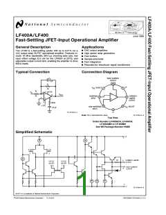
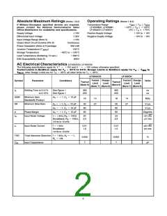
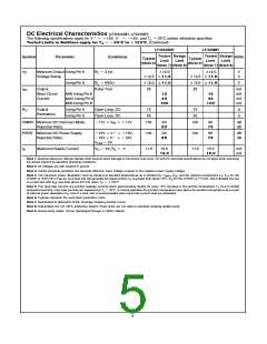
Absolute Maximum Ratings (Notes 1 ꢃ 2)
If MilitaryꢀAerospace specified devices are requiredꢂ
please contact the National Semiconductor Sales
OfficeꢀDistributors for availability and specificationsꢃ
Operating Ratings (Notes 1 ꢃ 2)
s
s
a
s
a
Temperature Range
LF400AMHꢂ LF400MH
LF400ACHꢂ LF400CH
T
MIN
55 C
T
A
T
MAX
A
s
s
b
T
A
125 C
ꢀ
ꢀ
s
0 C
ꢀ
T
70 C
ꢀ
a
b
a
g
g
g
Supply Voltage
18V
32V
16V
Positive Supply Voltage
Negative Supply Voltage
10V to 16V
b
10V to 16V
Differential Input Voltage
Input Voltage Range (Note 3)
Output Short Circuit Duration (Pin 6)
Power Dissipation (Note 4) H package
Continuous
500 mW
Junction Temperature (T
Storage Temperature
)
150 C
ꢀ
JMAX
b
a
65 C to 150 C
ꢀ
ꢀ
a
Lead Temperature (Solderingꢂ 10 secꢁ)
ESD Susceptibility (Note 9)
300 C
ꢀ
800V
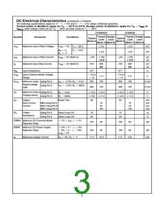
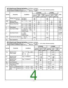
AC Electrical Characteristics (LF400ACHꢂ LF400CH)
b
The following specifications apply for Va
Tested Limits in Boldface apply for T
15V and V
15V unless otherwise specifiedꢁ
25 C to 95 Cꢀ Design Limits in Boldface apply for T
e a
e b
ꢀ
e
25 Cꢄ all other limits for T
e
T
to
MIN
ꢀ
J
A
e
e
25 Cꢁ
T
ꢄ other Design Limits are for T
ꢀ
ꢀ
MAX
A
J
LF400ACH
LF400CH
Tested Design
Tested Design
Symbol
Parameter
Conditions
Units
Typical
(Note 6)
Typical
(Note 6)
Limit
Limit
Limit
Limit
(Note 7) (Note 8)
(Note 7) (Note 8)
t
s
Settling Time to 0ꢁ01%
to 0ꢁ10%
SeeFigure 1
SeeFigure 1
365
200
365
200
ns
ns
e a
e
GBW
SR
Minimum Gain
A
1ꢂ C
10 pF
V
L
16
14
27
16
14
27
MHz
Bandwidth Product
e a
e b
e a
e
e
e
e
Minimum Slew Rate
A
A
A
1ꢂ C
10 pF
10 pF
10 pF
100X
30
60
60
30
60
60
Vꢀms
Vꢀms
v
L
1ꢂ C
V
V
L
w
Phase Margin
1ꢂ C
Degrees
L
e
Broadbandꢂ R
e
n
Input Noise Voltage
f
1 kHzꢂ R
23
23
nVꢀ Hz
0
S
e
100Xꢂ
2ꢁ3
2ꢁ3
mV rms
S
10 Hz to 10 kHz
e
Broadband
i
Input Noise Current
f
1 kHz
0ꢁ01
1ꢁ0
0ꢁ01
1ꢁ0
pAꢀ Hz
0
n
pA rms
10 Hz to 10 kHz
e
e b
1ꢂ
THD
Total Harmonic Distortion f
1 kHzꢂ A
V
0ꢁ002
7
0ꢁ002
7
%
e
R
10k
L
C
IN
Input Capacitance
pF
2

 NSC [ National Semiconductor ]