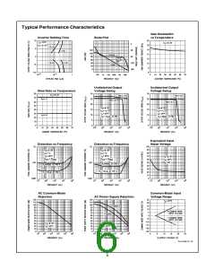
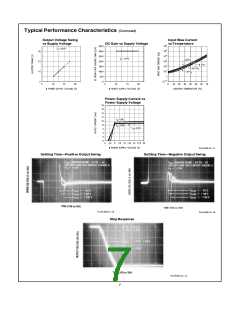
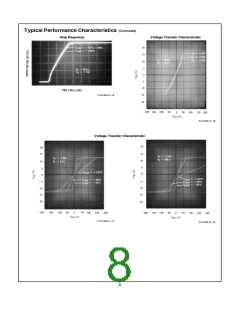
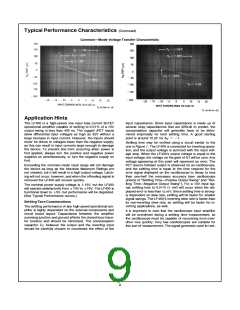
Typical Performance Characteristics (Continued)
CommonꢄMode Voltage Transfer Characteristic
TLꢀHꢀ9414–19
TLꢀHꢀ9414–20
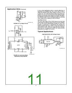
Application Hints
The LF400 is a high-speedꢂ low input bias current Bi-FET
operational amplifier capable of settling to 0ꢁ01% of a 10V
output swing in less than 400 nsꢁ The rugged JFET inputs
allow differential input voltages as high as 32V without a
large increase in input currentꢁ Howeverꢂ the inputs should
never be driven to voltages lower than the negative supplyꢂ
as this can result in input currents large enough to damage
the deviceꢁ To prevent this from occurring when power is
first appliedꢂ always turn the positive and negative power
supplies on simultaneouslyꢂ or turn the negative supply on
firstꢁ
input capacitanceꢁ Since input capacitance is made up of
several stray capacitances that are difficult to predictꢂ the
compensation capacitor will generally have to be deter-
mined empirically for best settling timeꢁ A good starting
e b
point is around 10 pF for A
1ꢁ
V
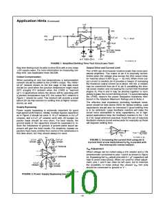
Settling time may be verified using a circuit similar to the
one inFigure 1ꢁ The LF400 is connected for inverting opera-
tionꢂ and the output voltage is summed with the input volt-
age stepꢁ When the LF400’s output voltage is equal to the
input voltageꢂ the voltage on the gate of Q1 will be zeroꢁ Any
voltage appearing at this point will represent an errorꢁ The
FET source follower output is observed on an oscilloscopeꢂ
and the settling time is equal to the time required for the
error signal displayed on the oscilloscope to decay to less
than one-half the necessary accuracy (see oscilloscope
photos of ‘‘Settling TimeꢅPositive Output Swing’’ and ‘‘Set-
tling TimeꢅNegative Output Swing’’)ꢁ For a 10V input sig-
nalꢂ settling time to 0ꢁ01% (1 mV) will occur when the dis-
played error is less than ꢀꢁꢂ mVꢁ Since settling time is strong-
ly dependent on slew rateꢂ settling will be faster for smaller
signal swingsꢁ The LF400’s inverting slew rate is faster than
its non-inverting slew rateꢂ so settling will be faster for in-
verting applicationsꢂ as wellꢁ
Exceeding the common-mode input range will not damage
the device as long as the Absolute Maximum Ratings are
not violatedꢂ but it will result in a high output voltageꢁ Latch-
ing will not occurꢂ howeverꢂ and when the offending signal is
removed the LF400 will recover quicklyꢁ
g
The nominal power supply voltage is 15Vꢂ but the LF400
g
g
will operate satisfactorily from 10V to 16Vꢁ The LF400 is
functional down to 5Vꢂ but performance will be degradedꢁ
g
(See Typical Performance curvesꢁ)
Settling Time Considerations
The settling performance of any high-speed operational am-
plifier is highly dependent on the external components and
circuit board layoutꢁ Capacitance between the amplifier
summing junction and ground affects the closed-loop trans-
fer function and should be minimizedꢁ The compensation
It is important to note that the oscilloscope input amplifier
will be overdriven during a settling time measurementꢂ so
the oscilloscope must be capable of recovering from over-
drive very quicklyꢁ Very few oscilloscopes are suitable for
this sort of measurementꢁ The signal generator used for set-
capacitor C between the output and the inverting input
C
should be carefully chosen to counteract the effect of the
9

 NSC [ National Semiconductor ]