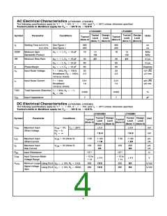
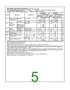
DC Electrical Characteristics (LF400ACHꢂ LF400CH)
b
The following specifications apply for Va
Tested Limits in Boldface apply for T
15V and V
15V unless otherwise specifiedꢁ
25 C to 95 Cꢀ Design Limits in Boldface apply for T
e a
e b
ꢀ
e
25 Cꢄ all other limits for T
e
T
to
MIN
ꢀ
J
A
e
e
T
ꢄ other Design Limits are for T
25 Cꢁ
ꢀ
ꢀ
MAX
A
J
LF400ACH
LF400CH
Tested Design
Tested Design
Symbol
Parameter
Conditions
Units
Typical
(Note 6)
Typical
(Note 6)
Limit
Limit
Limit
Limit
(Note 7) (Note 8)
(Note 7) (Note 8)
e
e
e
g
g
g
g
V
OS
Maximum Input Offset Voltage
V
0Vꢂ
T
T
25 C
ꢀ
0ꢁ5
2ꢁ0
3ꢁ0
5ꢁ0
mV
mV
CM
J
J
e
R
R
0ꢂ
70 C
ꢀ
S
e %
L
e
g
g
g
g
g
g
I
I
Maximum Input Offset Current
Maximum Input Bias Current
Input Resistance
V
0V (Note 5)
0V (Note 5)
50
100
50
100
pA
nA
OS
B
CM
CM
2ꢀ5
2ꢀ5
e
V
100
200
26
100
200
26
pA
nA
11
11
R
10
10
X
IN
b
a
b
12 to
a
14
V
CM
Input Common-Mode Voltage
Range
12 to
g
g
11
11
V
14
e
e
e
g
A
Minimum Large Using Pin 6
V
V
10Vꢂ R
10Vꢂ R
2 kX
300
100
100
300
100
100
VꢀmV
VꢀmV
VOL
O
L
Signal Voltage
e
g
Using Pin 8
600X
O
L
280
280
Gain
e
e
g
g
g
g
V
Minimum Output Using Pin 6
R
R
2 kX
12ꢁ5
12ꢁ0
25
12ꢁ0
11ꢁ0
12ꢁ5
12ꢁ0
25
12ꢁ0
11ꢁ0
V
V
O
L
Voltage Swing
Using Pin 8
g
g
g
g
600X
L
I
Output
Pulse Test
mA
mA
mA
mA
SC
Short Circuit
Current
MIN Using Pin 6
15
45
15
45
MAX Using Pin 6
MIN Using Pin 8
100
90
100
80
R
Output
Using Pin 6
Using Pin 8
Open Loopꢂ DC
Open Loopꢂ DC
75
50
75
50
X
X
O
Resistance
s
s
b
a
11V
CMRR Minimum DC Common Mode
Rejection Ratio
11V
V
IN
100
100
dB
a
s
s
s
s
a
b
a
PSRR Minimum DC Power Supply
Rejection Ratio
10V
V
V
15Vꢂ
b
b
15V
10Vꢂ
100
90
100
80
dB
e
V
0V
CM
e
e %
0Vꢂ R
L
I
Maximum Supply Current
V
O
11ꢁ0
13ꢁ0
11ꢁ0
13ꢁ0
mA
S
3

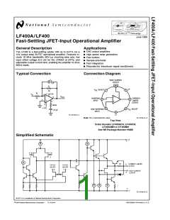
 NSC [ National Semiconductor ]