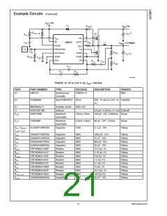
Application Information (Continued)
as high as possible. Two zeroes fZ1 and fZ2 are placed at the
double pole frequency to cancel the double pole phase lag.
Then, a pole, fP1 is placed at the frequency of the ESR zero.
A final pole fP2 is placed at one-half of the switching fre-
quency. The gain of the error amplifier transfer function is
selected to give the best bandwidth possible without violat-
ing the Nyquist stability criteria. In practice, a good crossover
point is one-fifth of the switching frequency, or 60 kHz for this
example. The generic equation for the error amplifier transfer
function is:
20150974
In this equation the variable AEA is a ratio of the values of the
capacitance and resistance of the compensation compo-
nents, arranged as shown in Figure 13. AEA is selected to
provide the desired bandwidth. A starting value of 80,000 for
AEA should give a conservative bandwidth. Increasing the
value will increase the bandwidth, but will also decrease
phase margin. Designs with 45-60˚ are usually best because
they represent a good trade-off between bandwidth and
phase margin. In general, phase margin is lowest and gain
highest (worst-case) for maximum input voltage and mini-
mum output current. One method to select AEA is to use an
iterative process beginning with these worst-case conditions.
1. Increase AEA
2. Check overall bandwidth and phase margin
3. Change VIN to minimum and recheck overall bandwidth
and phase margin
20150975
4. Change IO to maximum and recheck overall bandwidth
and phase margin
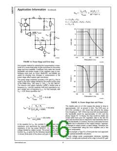
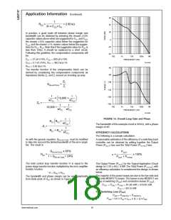
FIGURE 15. Error Amp. Gain and Phase
The process ends when the both bandwidth and the phase
margin are sufficiently high. For this example input voltage
can vary from 3.0 to 3.6V and output current can vary from 0
to 4A, and after a few iterations a moderate gain factor of
101dB is used.
In VM regulators, the top feedback resistor RFB2 forms a part
of the compensation. Setting RFB2 to 10 kΩ 1%, usually
gives values for the other compensation resistors and ca-
>
pacitors that fall within a reasonable range. (Capacitances
<
1 pF, resistances 1 MΩ) CC1, CC2, CC3, RC1, and RC2 are
selected to provide the poles and zeroes at the desired
frequencies, using the following equations:
The error amplifier of the LM2747 has a unity-gain band-
width of 9 MHz. In order to model the effect of this limitation,
the open-loop gain can be calculated as:
The new error amplifier transfer function that takes into
account unity-gain bandwidth is:
The gain and phase of the error amplifier are shown in
Figure 15.
17
www.national.com

 NSC [ National Semiconductor ]