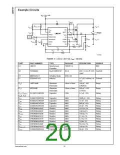
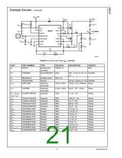
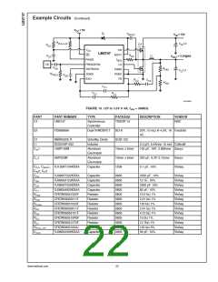
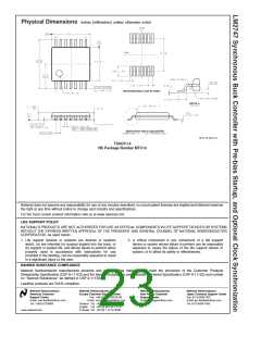
Application Information (Continued)
PSW = 0.5 x 3.3V x 4A x 300 kHz x 31 ns
PSW = 61.38 mW
Here n is the number of paralleled capacitors, ESR is the
equivalent series resistance of each, and PCAP is the dissi-
pation in each. So for example if we use only one input
capacitor of 24 mΩ.
The FDS6898A has a typical turn-on rise time tr and turn-off
fall time tf of 15 ns and 16 ns, respectively. The switching
losses for this type of dual N-Channel MOSFETs are
0.061W.
FET Conduction Loss (PCND
PCND = PCND1 + PCND2
PCND1 = I2
x RDS(ON) x k x D
)
OUT
PCND2 = I2
x RDS(ON) x k x (1-D)
OUT
PCAP = 88.8 mW
RDS(ON) = 13 mΩ and the factor is a constant value (k = 1.3)
to account for the increasing RDS(ON) of a FET due to heat-
ing.
Output Inductor Loss (PIND
)
PIND = I2
x DCR
OUT
PCND1 = (4A)2 x 13 mΩ x 1.3 x 0.364
PCND2 = (4A)2 x 13 mΩ x 1.3 x (1 - 0.364)
PCND = 98.42 mW + 172 mW = 270.42 mW
There are few additional losses that are taken into account:
IC Operating Loss (PIC)
where DCR is the DC resistance. Therefore, for example
PIND = (4A)2 x 11 mΩ
PIND = 176 mW
Total System Efficiency
PTOTAL = PFET + PIC + PGATE + PCAP + PIND
PIC = IQ_VCC x VCC
,
where IQ-VCC is the typical operating VCC current
PIC= 1.7 mA x 3.3V = 5.61 mW
FET Gate Charging Loss (PGATE
)
PGATE = n x VCC x QGS x fSW
PGATE = 2 x 3.3V x 3 nC x 300 kHz
PGATE = 5.94 mW
The value n is the total number of FETs used and QGS is the
typical gate-source charge value, which is 3 nC. For the
FDS6898A the gate charging loss is 5.94 mW.
Input Capacitor Loss (PCAP
)
where,
19
www.national.com

 NSC [ National Semiconductor ]