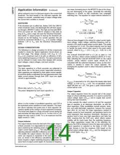
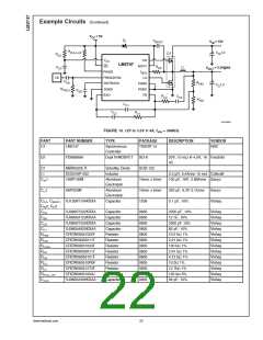
Application Information (Continued)
In practice, a good trade off between phase margin and
bandwidth can be obtained by selecting the closest 10%
capacitor values above what are suggested for CC1 and CC2
,
the closest 10% capacitor value below the suggestion for
CC3, and the closest 1% resistor values below the sugges-
tions for RC1, RC2. Note that if the suggested value for RC2 is
less than 100Ω, it should be replaced by a short circuit.
Following this guideline, the compensation components will
be:
CC1 = 27 pF 10%, CC2 = 820 pF 10%
CC3 = 2.7 nF 10%, RC1 = 39.2 kΩ 1%
RC2 = 2.55 kΩ 1%
20150985
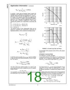
The transfer function of the compensation block can be
derived by considering the compensation components as
impedance blocks ZF and ZI around an inverting op-amp:
20150986
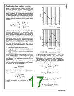
FIGURE 16. Overall Loop Gain and Phase
The bandwidth of this example circuit is 59 kHz, with a phase
margin of 60˚.
EFFICIENCY CALCULATIONS
The following is a sample calculation.
As with the generic equation, GEA-ACTUAL must be modified
to take into account the limited bandwidth of the error ampli-
fier. The result is:
A reasonable estimation of the efficiency of a switching buck
controller can be obtained by adding together the Output
Power (POUT) loss and the Total Power (PTOTAL) loss:
The total control loop transfer function H is equal to the
power stage transfer function multiplied by the error amplifier
transfer function.
The Output Power (POUT) for the Typical Application Circuit
design is (1.2V x 4A) = 4.8W. The Total Power (PTOTAL), with
an efficiency calculation to complement the design, is shown
below.
H = GPS x HEA
The majority of the power losses are due to the low side and
high side MOSFET’s losses. The losses in any MOSFET are
group of switching (PSW) and conduction losses (PCND).
The bandwidth and phase margin can be read graphically
from Bode plots of HEA as shown in Figure 16.
PFET = PSW + PCND = 61.38 mW + 270.42 mW
PFET = 331.8 mW
FET Switching Loss (PSW
)
PSW = PSW(ON) + PSW(OFF)
PSW = 0.5 x VIN x IOUT x (tr + tf) x fSW
www.national.com
18

 NSC [ National Semiconductor ]