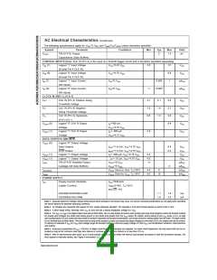
AC Electrical Characteristics (Continued)
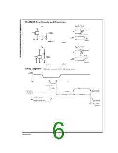
Note 7: The CS input is assumed to bracket the WR strobe input and therefore timing is dependent on the WR pulse width. An arbitrarily wide pulse width will hold
the converter in a reset mode and the start of conversion is initiated by the low to high transition of the WR pulse (see timing diagrams).
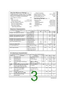
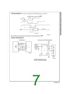
Note 8: None of these A/Ds requires a zero adjust (see section 2.5.1). To obtain zero code at other analog input voltages see section 2.5 and Figure 7.
Note 9: The V
/2 pin is the center point of a two-resistor divider connected from V to ground. In all versions of the ADC0801, ADC0802, ADC0803, and
CC
REF
ADC0805, and in the ADC0804LCJ, each resistor is typically 16 kΩ. In all versions of the ADC0804 except the ADC0804LCJ, each resistor is typically 2.2 kΩ.
Note 10: Human body model, 100 pF discharged through a 1.5 kΩ resistor.
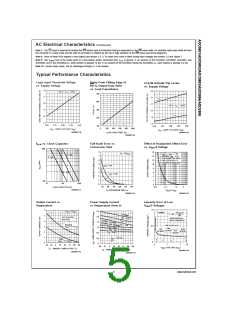
Typical Performance Characteristics
Logic Input Threshold Voltage
vs. Supply Voltage
Delay From Falling Edge of
RD to Output Data Valid
vs. Load Capacitance
CLK IN Schmitt Trip Levels
vs. Supply Voltage
DS005671-38
DS005671-40
DS005671-39
fCLK vs. Clock Capacitor
Full-Scale Error vs
Conversion Time
Effect of Unadjusted Offset Error
vs. VREF/2 Voltage
DS005671-41
DS005671-42
DS005671-43
Output Current vs
Temperature
Linearity Error at Low
VREF/2 Voltages
Power Supply Current
vs Temperature (Note 9)
DS005671-46
DS005671-44
DS005671-45
5
www.national.com

 NSC [ National Semiconductor ]