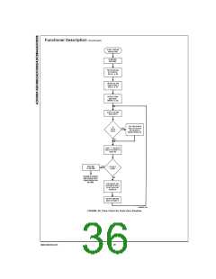
Functional Description (Continued)
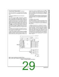
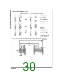
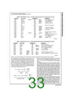
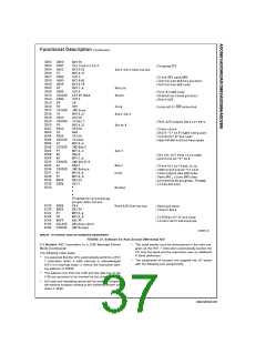
SAMPLE PROGRAM FOR Figure 17 INTERFACING MULTIPLE A/D’s IN AN MC6800 SYSTEM
DS005671-A3
SAMPLE PROGRAM FOR Figure 17 INTERFACING MULTIPLE A/D’s IN AN MC6800 SYSTEM
DS005671-A4
Note 25: In order for the microprocessor to service subroutines and interrupts, the stack pointer must be dimensioned in the user’s program.
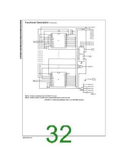
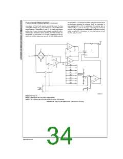
For amplification of DC input signals, a major system error is
the input offset voltage of the amplifiers used for the preamp.
Figure 18 is a gain of 100 differential preamp whose offset
voltage errors will be cancelled by a zeroing subroutine
which is performed by the INS8080A microprocessor sys-
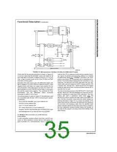
where IX is the current through resistor RX. All of the offset
=
±
error terms can be cancelled by making IXRX VOS1
VOS3 VOS2. This is the principle of this auto-zeroing
scheme.
+
−
The INS8080A uses the 3 I/O ports of an INS8255 Program-
able Peripheral Interface (PPI) to control the auto zeroing
and input data from the ADC0801 as shown in Figure 19.
The PPI is programmed for basic I/O operation (mode 0) with
Port A being an input port and Ports B and C being output
ports. Two bits of Port C are used to alternately open or close
the 2 switches at the input of the preamp. Switch SW1 is
closed to force the preamp’s differential input to be zero dur-
ing the zeroing subroutine and then opened and SW2 is then
closed for conversion of the actual differential input signal.
Using 2 switches in this manner eliminates concern for the
ON resistance of the switches as they must conduct only the
input bias current of the input amplifiers.
tem. The total allowable input offset voltage error for this
1
preamp is only 50 µV for
⁄4 LSB error. This would obviously
require very precise amplifiers. The expression for the differ-
ential output voltage of the preamp is:
Output Port B is used as a successive approximation regis-
ter by the 8080 and the binary scaled resistors in series with
each output bit create a D/A converter. During the zeroing
subroutine, the voltage at Vx increases or decreases as re-
quired to make the differential output voltage equal to zero.
This is accomplished by ensuring that the voltage at the out-
put of A1 is approximately 2.5V so that a logic “1” (5V) on
33
www.national.com

 NSC [ National Semiconductor ]