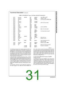
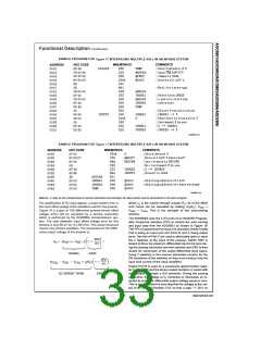
Functional Description (Continued)
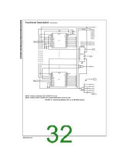
DS005671-92
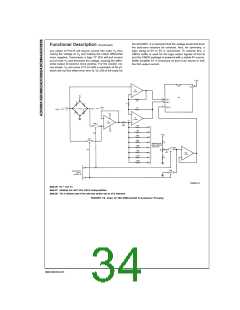
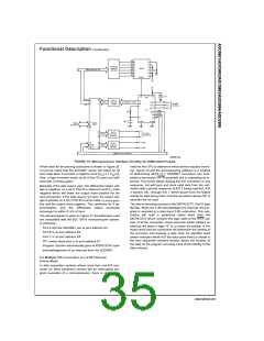
FIGURE 19. Microprocessor Interface Circuitry for Differential Preamp
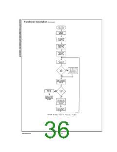
A flow chart for the zeroing subroutine is shown in Figure 20.
It must be noted that the ADC0801 series will output an all
zero code when it converts a negative input [VIN(−) ≥ VIN(+)].
Also, a logic inversion exists as all of the I/O ports are buff-
ered with inverting gates.
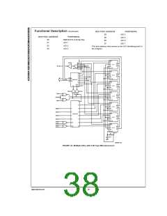
need for the CPU to determine which device requires servic-
ing. Figure 22 and the accompanying software is a method
of determining which of 7 ADC0801 converters has com-
pleted a conversion (INTR asserted) and is requesting an in-
terrupt. This circuit allows starting the A/D converters in any
sequence, but will input and store valid data from the con-
verters with a priority sequence of A/D 1 being read first, A/D
2 second, etc., through A/D 7 which would have the lowest
priority for data being read. Only the converters whose INT is
asserted will be read.
Basically, if the data read is zero, the differential output volt-
age is negative, so a bit in Port B is cleared to pull VX more
negative which will make the output more positive for the
next conversion. If the data read is not zero, the output volt-
age is positive so a bit in Port B is set to make VX more posi-
tive and the output more negative. This continues for 8 ap-
proximations and the differential output eventually
converges to within 5 mV of zero.
The key to decoding circuitry is the DM74LS373, 8-bit D type
flip-flop. When the Z-80 acknowledges the interrupt, the pro-
gram is vectored to a data input Z-80 subroutine. This sub-
routine will read
a peripheral status word from the
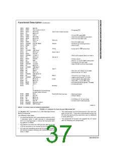
The actual program is given in Figure 21. All addresses used
are compatible with the BLC 80/10 microcomputer system.
In particular:
DM74LS373 which contains the logic state of the INTR out-
puts of all the converters. Each converter which initiates an
interrupt will place a logic “0” in a unique bit position in the
status word and the subroutine will determine the identity of
the converter and execute a data read. An identifier word
(which indicates which A/D the data came from) is stored in
the next sequential memory location above the location of
the data so the program can keep track of the identity of the
data entered.
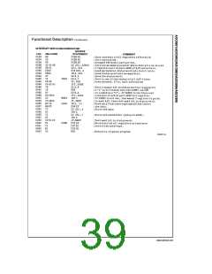
Port A and the ADC0801 are at port address E4
Port B is at port address E5
Port C is at port address E6
PPI control word port is at port address E7
Program Counter automatically goes to ADDR:3C3D upon
acknowledgement of an interrupt from the ADC0801
5.3 Multiple A/D Converters in a Z-80 Interrupt
Driven Mode
In data acquisition systems where more than one A/D con-
verter (or other peripheral device) will be interrupting pro-
gram execution of a microprocessor, there is obviously a
35
www.national.com

 NSC [ National Semiconductor ]