Nexperia
XC7SH86
2-input EXCLUSIVE-OR gate
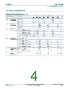
11. Dynamic characteristics
Table 8. Dynamic characteristics
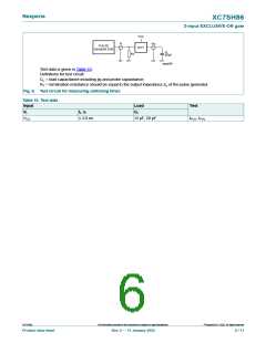
GND = 0 V. For waveform see Fig. 5. For test circuit see Fig. 6.
Symbol Parameter Conditions
25 °C
Min Typ Max
-40 °C to +85 °C -40 °C to +125 °C Unit
Min
Max
Min
Max
tpd
propagation A and B to Y
delay
[1]
[2]
VCC = 3.0 V to 3.6 V
CL = 15 pF
-
-
4.0 11.0
5.8 14.5
1.0
1.0
13.0
16.5
1.0
1.0
14.0
18.5
ns
ns
CL = 50 pF
VCC = 4.5 V to 5.5 V
CL = 15 pF
[3]
[4]
-
-
-
3.4
4.9
9
6.8
8.8
-
1.0
1.0
-
8.0
10.0
-
1.0
1.0
-
8.5
11.5
-
ns
ns
pF
CL = 50 pF
CPD
power
per buffer; CL = 50 pF;
f = 1 MHz;
dissipation
capacitance VI = GND to VCC
[1] tpd is the same as tPLH and tPHL
.
[2] Typical values are measured at VCC = 3.3 V.
[3] Typical values are measured at VCC = 5.0 V.
[4] CPD is used to determine the dynamic power dissipation PD (μW).
PD = CPD × VCC 2 × fi + ∑(CL × VCC 2 × fo) where:
fi = input frequency in MHz;
fo = output frequency in MHz;
CL = output load capacitance in pF;
VCC = supply voltage in V.
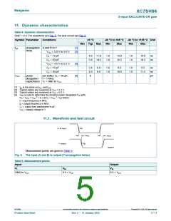
11.1. Waveform and test circuit
V
M
A, B input
t
t
PHL
PLH
V
Y output
M
mna041
Measurement points are given in Table 9.
Fig. 5. The input (A and B) to output (Y) propagation delays
Table 9. Measurement points
Input
Output
VM
0.5 × VCC
VI
VM
GND to VCC
0.5 × VCC
©
XC7SH86
All information provided in this document is subject to legal disclaimers.
Nexperia B.V. 2022. All rights reserved
Product data sheet
Rev. 2 — 11 January 2022
5 / 11

 NEXPERIA [ Nexperia ]