Nexperia
XC7SH86
2-input EXCLUSIVE-OR gate
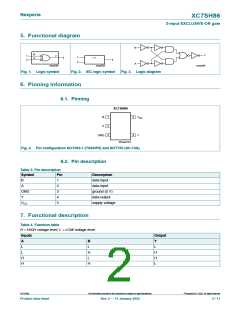
5. Functional diagram
B
B
Y
1
2
Y
1
2
4
= 1
A
4
A
mna038
mna039
mna040
Fig. 1. Logic symbol
Fig. 2. IEC logic symbol
Fig. 3. Logic diagram
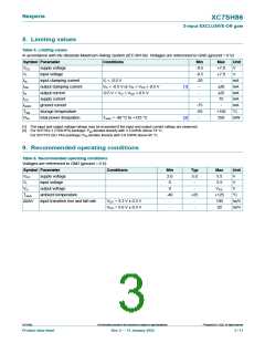
6. Pinning information
6.1. Pinning
XC7SH86
1
2
3
5
4
B
A
V
Y
CC
GND
001aak133
Fig. 4. Pin configuration SOT353-1 (TSSOP5) and SOT753 (SC-74A)
6.2. Pin description
Table 3. Pin description
Symbol
Pin
1
Description
data input
B
A
2
data input
GND
Y
3
ground (0 V)
data output
supply voltage
4
VCC
5
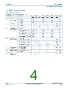
7. Functional description
Table 4. Function table
H = HIGH voltage level; L = LOW voltage level.
Inputs
Output
A
L
B
L
Y
L
L
H
L
H
H
L
H
H
H
©
XC7SH86
All information provided in this document is subject to legal disclaimers.
Nexperia B.V. 2022. All rights reserved
Product data sheet
Rev. 2 — 11 January 2022
2 / 11

 NEXPERIA [ Nexperia ]